You are currently viewing SemiWiki as a guest which gives you limited access to the site. To view blog comments and experience other SemiWiki features you must be a registered member. Registration is fast, simple, and absolutely free so please,
join our community today!
September WSTS data shows the 3Q 2012 semiconductor market increased 1.8% from 2Q 2012. The year 2012 semiconductor market will certainly show a decline. 4Q 2012 would need to grow 11% to result in positive growth for 2012. The outlook for key semiconductor companies points to a 4Q 2012 roughly flat with 3Q 2012. The table below shows… Read More
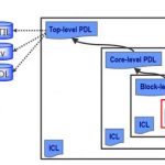
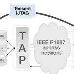
Until now, the integration and testing of IP blocks used in large SOCs has been a manual, time consuming design effort. A new standard called IEEE P1687 (or “IJTAG”) for IP plug-and-play integration is emerging to simplify these tasks. EDA tools are also emerging to support the new standard. Last week mentor announcedTessent IJTAG,… Read More
I attended the Jasper User Group this week, at least the keynotes, the first by Kathryn Kranen the CEO of Jasper and the second by Bob Bentley of Intel.
Kathryn went over some history, going back to when the company was started (under the name Tempus Fugit) back in August 2002 with a single product for protocol verification. Now, since… Read More
One technology that has quietly gone mainstream in semiconductor design is FPGA prototyping. That is, using an FPGA version of the design to run extensive verification. There are two approaches to doing this. The first way is simply to build an prototype board, buy some FPGAs from Xilinx or Altera and do everything yourself. The… Read More
Analog Mixed-Signal (AMS) behavioral models have not caught on with the AMS designer community. Why? I suspect a significant reason (but certainly not the only one) is the way they are presented.
First, what is AMS behavioral modeling?
I define it as “a set of user-defined equations that decribe the terminal behavior of a component”.… Read More
Modern SoC (System On Chip) designs contain a larger number of RAM (Random Access Memory) instances, so how do you know what the speed, timing and power are for any instance? There are a couple of approaches:
[LIST=1]
Trust the IP supplier to give you models that use polynomial equations to curve-fit the performance numbers based…
Read More
The numbers for smartphone sales in Q3 are starting to roll in. These are in units and not yet revenue (let alone profit) numbers although everyone down to Sony is for sure profitable. Samsung is running away with the volume, selling more than Apple, Huawei and Sony put together. One name that is missing is Motorola (Google) which … Read More
At ICCAD earlier this week, CEDA sponsored a talk by Alberto Sangiovanni-Vincentelli looking back over the last 30 years (it is the 30th anniversary of ICCAD) and looking to the future. As is always the case in these sorts of presentations, the retrospective contained a lot more detail than the going forward part. Clayton Christensen… Read More
Test is the Rodney Dangerfield of EDA, it doesn’t get any respect. All designs need to be tested but somehow synthesis, routing, analog layout and the rest are the sexy areas. In my spoof all purpose EDA keynote address I even dissed it:You are short on time so slip in a quick mention of manufacturing test. Who knows anything … Read More
Solido Design Automation and TSMC recently published an article in EE Times describing how Solido’s High-Sigma Monte Carlo tool is used with TSMC PDK’s to achieve high-yield, high-performance memory design. This project has been a big part of my life for the past three years and it is time for a victory lap!
In TSMC 28nm, 20nm and … Read More