You are currently viewing SemiWiki as a guest which gives you limited access to the site. To view blog comments and experience other SemiWiki features you must be a registered member. Registration is fast, simple, and absolutely free so please,
join our community today!
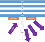
EUV (Extreme UltraViolet) lithography has received attention within the semiconductor industry since its development inception in 1997 with the formation of the EUV LLC [1], and more recently, since the 7nm node began, with limited use by Samsung and TSMC being touted as key advantages [2, 3]. As with any key critical technology,
…
Read More
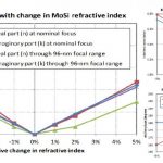
Let’s start with the bottom line: in 14nm processes, errors which have typically been little more than noise with respect to photomask critical dimension (CD) control targets at larger process nodes are about to become very significant, even out of control if not accounted for.… Read More