My first transistor-level IC design job was with Intel, doing DRAM designs by shrinking the layout to a smaller process node, and it also required running lots of SPICE runs with manually extracted parasitics to verify that everything was operating OK, meeting the access time specifications and power requirements across PVT … Read More
Tag: layout-dependent effects
How ST Designs with Layout Dependent Effects (LDE)
I first visited STat their Agrate, Italy site where Flash memory development is done. At DACthis year Antonio Bogani talked about how ST designs with LDE while using EDA tools and a PDK (Process Design Kit) from Cadence. They recorded the 17 minute presentation, and you can view it herewithout having to register. Antonio’s… Read More
Custom Physical IC Design update from Cadence
Custom IC design and layout is becoming more difficult at 20nm and smaller nodes, so the EDA tools have to get smarter and work harder for us in order to maintain productivity with the fewest iterations to reach our specs. Dave Stylesand John Stabenow of Cadence met with me last Monday in Austin at the DAC exhibit area.
John Stabenow… Read More
Variation-aware IC Design
We’ve blogged before about Layout Dependent Effects (LDE) on SemiWiki and how it further complicates the IC design and layout process, especially at 28nm and lower nodes because the IC layout starts to change the MOS device performance. There’s an interesting webinarfrom Cadence on Variation-aware IC Design, … Read More
When the lines on the roadmap get closer together
Tech aficionados love roadmaps. The confidence a roadmap instills – whether using tangible evidence or just a good story – can be priceless. Decisions on “the next big thing”, sometimes years and a lot of uncertain advancements away, hinge on the ability of a technology marketing team to define and communicate a roadmap.
Any roadmap… Read More
Cadence at 20nm
Cadence has a new white paper out about the changes in IC design that are coming at 20nm. One thing is very clear: 20nm is not simply “more of the same”. All design, from basic standard cells up to huge SoCs has several new challenges to go along with all the old ones that we had at 45nm and 28nm.
I should emphasize that the paper… Read More
TSMC Theater Presentation: Ciranova!
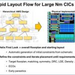
Ciranova presented a hierarchical custom layout flow used on several large advanced-node designs to reduce total layout time by about 50%. Ciranova itself does automated floorplanning and placement software with only limited routing; but since the first two constitute the majority of custom layout time, and strongly influence… Read More
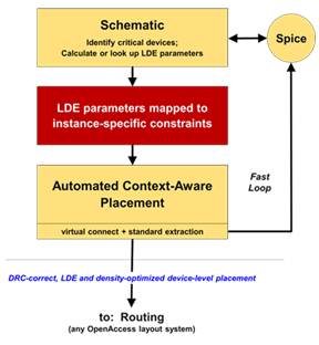
A Simple, Scalable LDE Optimization Flow for 28/20nm Custom/AMS Design
At 28nm and below, a number of electrical variation effects become significant which depend not only on individual devices, but the physical interaction between neighboring devices, wells, etc during the manufacturing process. Some of these effects have become collectively referred to as “Layout Dependent Effects” (LDE);… Read More
iLVS: Improving LVS Usability at Advanced Nodes
LVS Challenges at Advanced Nodes
Accurate, comprehensive device recognition, connectivity extraction, netlist generation and, ultimately, circuit comparison becomes more complex with each new process generation. As the number of layers and layer derivations increases the complexity of devices, especially Layout Dependent… Read More


