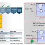
RTL Design For Power

RTL Design For Power
by Daniel Payne on 08-11-2013 at 2:25 pm

My Samsung Galaxy Note II lasts about two days on a single battery charge, which is quite the improvement from the Galaxy Note I with only a one day battery charge. Mobile SoCs are being constrained by battery life limitations, and consumers love longer-laster devices.

There are at least two approaches to Design For Power:

  • Gate-level
Read More

Full Chip IR Drop Analysis using Distributed Multi Processing

Full Chip IR Drop Analysis using Distributed Multi Processing
by Daniel Payne on 07-02-2013 at 6:56 pm

IR drop analysis across your board, package and SoC ensures that your Power Delivery Network (PDN) is robust, and that your system will function to spec. There are both static and dynamic approaches to IR drop analysis of a full-chip with billions of transistors, while the dynamic approach produces the most accurate results compared… Read More


Transistor, Gate and RTL Debug Update at DAC

Transistor, Gate and RTL Debug Update at DAC
by Daniel Payne on 05-29-2013 at 10:53 am

Debugging an IC design at the transistor, Gate and RTL levels is often necessary to meet timing requirements and understand analog or digital behavior, yet the process itself can be a tedious one, filled with manual steps, therefore making it an error-prone process. EDA tools have been created to help us graphically debug transistor,… Read More


Enabling 14nm FinFET Design

Enabling 14nm FinFET Design
by Daniel Payne on 05-28-2013 at 12:54 pm

There’s never a dull moment in the foundry race to offer FinFET processes that enable leading-edge SoC design. Today I attended a webinar hosted by Samsung and Synopsys on how to enable 14nm FinFET design. The two speakers were Dr. Kuang-Kuo Lin from Samsung and Dr. Henry Sheng from Synopsys.


Dr. Kuang-Kuo Lin, Samsung


Dr.Read More