You are currently viewing SemiWiki as a guest which gives you limited access to the site. To view blog comments and experience other SemiWiki features you must be a registered member. Registration is fast, simple, and absolutely free so please,
join our community today!
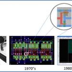
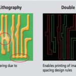
Have you seen the latest design rule manuals? At 28nm and 20nm design sign-off is no longer just DRC and LVS. These basic components of physical verification are being augmented by an expansive set of yield analysis and critical feature identification capabilities, as well as layout enhancements, printability, and performance… Read More
Matt Elmore of ANSYS/Apache has an interesting blog posting about thermal analysis in 3D integrated circuits. With both technical and economic challenges at process nodes as we push below 28nm, increasingly product groups are looking towards through-silicon-via (TSV) based approaches as a way of keeping Moore’s law… Read More
Last month at DAC I learned how IBM, Cadence, ARM, GLOBALFOUNDRIES and Samsung approach the challenges of SoC design, EDA design and fabrication at the 20nm node. Today I followed up by reading a white paper on 20nm IC design challenges authored by Cadence, a welcome relief to the previous marketing mantra of EDA 360.
Here’s… Read More
Over the years many attempts have been made to increase the level of automation in analog design. Most of these have not been especially successful. Probably part of the reason was inadequate technology but also there is an attitude that “real” analog designers design polygons on the bare silicon. I think two things… Read More
There is an interesting Gizmodo review of an HTC Android-based smartphone. The basically positive review (as good as the iPhone, best Android phone at the time) ends up with an update:UPDATE: After more extensive testing there’s something a little weird going on. You’ll probably only see this while gaming, but there’s… Read More
The 1st Atrenta Technology Forum in Japan (well, it used to be the user group meeting, so it’s only the first in a very technical sense) is next week on July 19th from 1pm until 5.15pm. It will be held in the Shin-Yokohama Kokusai Hotel (how to access it here).
In the unlikely event that non-Japanese are reading this blog, here’s… Read More
I attended the Synopsys webinar today for a tool called Custom Explorer Ultra (CXU). Product details on the Synopsys web site are here. The CXU tool would be used by AMS designers that want to setup, control and view results from simulators like HSPICE, CustomSim or VCS on transistor-level and AMS designs.… Read More
As 2D device scaling becomes impractical, 3D-IC integration is emerging as the natural evolution of semiconductor technology; it is the convergence of performance, power and functionality. Some of the benefits of 3D-IC, such as increasing complexity, improved performance, reducing power consumption and decreasing footprints,… Read More
If you are in Asia then the Synopsys user group SNUG is coming up, soon in Japan and next month in China. Actually if you are in India I’m afraid you already missed it last month, just after DAC.
SNUG Japan is on 12th July in a couple of days time from 10am until 8pm in Tokyo.
In China there are 3 between August 14th and 21st
…
Read More
Formal Going Mainstreamby Paul McLellan on 07-10-2012 at 7:29 pmCategories: EDA
In Mike Muller’s keynote at DAC he wanted to make formal approaches an integral part of writing RTL. After all, formal captures design intent and then, at least much of the time, can verify whether the RTL written actually matches that intent. Today, formal is not used that way and is typically something served “on the side” by specialist… Read More