You are currently viewing SemiWiki as a guest which gives you limited access to the site. To view blog comments and experience other SemiWiki features you must be a registered member. Registration is fast, simple, and absolutely free so please,
join our community today!
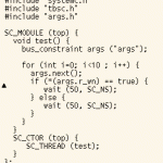
As more people adopt high-level synthesis (HLS) they start to worry about what is the best design flow to be using. This is especially so for verification since it forms such a large part of the effort on a modern SoC. The more people rely on HLS for producing their RTL from C, the more they realize they had better do a good job of verifying… Read More
Increasingly, end users in some markets are requiring soft error rate (SER) data. This is a measure of how resistant the design (library, chip, system) is to single event effects (SEE). These manifest themselves as SEU (upset), SET (transient), SEL (latch-up), SEFI (functional interrupt).
There are two main sources that cause… Read More
Remember? During DAC2013 I talked about a new kind of innovation: A Virtual Fabrication Platform, SEMulator3D, developed by COVENTOR. Now, to my pleasant surprise, there is something to report on the proven results from this platform. IBM, in association with COVENTOR, has successfully implemented a 3D Virtual Fabrication… Read More
For decades we have used a model of faults in chips that assumes that a given signal is stuck-at-0 or stuck-at-1. And when I say decades, I mean it. The D-algorithm was invented at IBM in 1966, the year after Gordon Moore made a now very famous observation about the number of transistors on an integrated circuit. We know that stuck-at… Read More
Layout editing is a complex task, traditionally done manually by designers, and the layout design productivity largely depends on the designer’s skills and expertise. However, a good tool with features for ease of design is a must. Layout productivity has been an area of focus and various features are constantly being added in… Read More
You can only design and optimize for low-power SoC designs if you can actually simulate the entire Chip, Package and System together. The engineers at ANSYS-Apachehave figured out how to do that and talked about their design for power methodology in a webinar today. I listened to Arvind Shanmugavel present a few dozen slides and… Read More
Must See SoC IP!by Daniel Nenni on 09-02-2013 at 5:30 pmCategories: IP
IP is the center of the semiconductor universe and nobody knows this better than Design and Reuse. The D&R website was launched in 1997 targeting the emerging commercial semiconductor IP market. Today, with more than 15,000 IP/SOC product descriptions updated daily, D&R is the #1 IP site matching customer requirements… Read More
One of the challenges in doing a complex analog or mixed signal design is that things get out of step. One designer is tweaking the schematic and re-simulating, another is tweaking the layout of transistors, another is changing the routing. This is not because the design flow is messed up, but rather it reflects reality. If you wait… Read More
The history of TSMC and its Open Innovation Platform (OIP) is, like almost everything in semiconductors, driven by the economics of semiconductor manufacturing. Of course ICs started 50 years ago at Fairchild (very close to where Google is headquartered today, these things go in circles). The planarization approach, whereby… Read More
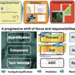
Here, I am talking about reliability of chip design in the context of electrical effects, not external factors like cosmic rays. So, the electrical factors that could affect reliability of chips could be excessive power dissipation, noise, EM (Electromigration), ESD (Electrostatic Discharge), substrate noise coupling and… Read More