




When I first heard about a foundry possibly licensing FD-SOI I would have bet it was SMIC in China. What better market for a low cost, low power, easy to manufacture alternative to FinFETs? The foundry of course was Samsung which also made complete sense since they have 28nm gate-first capacity that matches up nicely to 28nm FD-SOI.… Read More

Tag: eda
Dr. Evil and On-Chip "LASERS" for Silicon Photonics
In the 1999 comedy, The Spy Who Shagged Me, Dr. Evil laments about why he can’t have sharks with “laser beams” attached to their heads. I get the feeling that silicon photonic designers sometimes feel the same way about why they don’t yet have integrated on-chip laser light sources. While off-chip light… Read More
3D TCAD Simulation of Silicon Power Devices
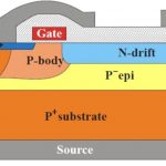
Process and device engineers are some of the unsung heroes in our semiconductor industry that have the daunting task of figuring out how to actually create a new process node that will fit some specific, market niche with sufficient yield to make their companies profitable and stand out from the competition. One such market segment… Read More
The Most Important Point You May Have Missed at CDNLive 2016!
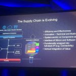
This was the best keynote lineup I can remember at a user group meeting. All four speakers are visionaries but from very different perspectives. The video of the event will be up later this month but from my first count the word “System(s)” was mentioned 32 times and the underlying message will transform the semiconductor industry… Read More
PCB Design Requires Both Speed and Accuracy of SI/PI Analysis

The prevailing industry trends are clear: (1) PCB and die package designs are becoming more complex, across both mobile and high-performance applications; (2) communication interface performance between chips (and their related protocols) is increasingly demanding to verify; (3) signal integrity and power integrity issues… Read More
IoT Prototyping Workshop in Monterey CA!
With the coming onslaught of IoT designs from big companies and small, the opportunity for IoT FPGA prototyping deserves a closer look. This session will start off with a keynote “The Internet of Trust and a New Frontier For Exploration” and will be followed by a discussion with industry experts Don Dingee, Frank Schirrmeister,… Read More
In the Valley & thinking about FD-SOI for your next chip design? Epic (and free) symposium 13 April
If you’re in the chip biz in Silicon Valley, check out the SOI Consortium FD-SOI Symposium on April 13th in San Jose. They’ve been running these things since 2009, and I have to say that this one is the most comprehensive to date. Headliners include Cisco, Sony, NXP, SigmaDesigns, ARM, Ciena plus the big FD-SOI foundries,… Read More
The Latest in Static Timing Analysis with Variation Modeling
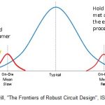
In many ways, static timing analysis (STA) is more of an art than a science. Methodologists are faced with addressing complex phenomena that impact circuit delay — e.g., signal crosstalk, dynamic I*R supply voltage drop, temperature inversion, device aging effects, and especially (correlated and uncorrelated) process… Read More
What SOC Size Growth Means for IP Management
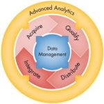
Whether or not in the past you believed all the of rhetoric about exploding design complexity in SOC’s, today there can be no debate that SOC size and complexity is well beyond something that can be managed without some kind of design management system. As would be expected, development of most larger designs relies on a data management… Read More
Cadence is again the best EDA company to work for!

We wrote about the history of Cadence in preparation for our book “Fabless: The Transformation of the Semiconductor Industry” in 2012. EDA played a key role in enabling the fabless semiconductor revolution and Cadence was right there at the beginning. Famed EETimes editor Richard Goering helped us with the book and the Cadence… Read More