You are currently viewing SemiWiki as a guest which gives you limited access to the site. To view blog comments and experience other SemiWiki features you must be a registered member. Registration is fast, simple, and absolutely free so please,
join our community today!
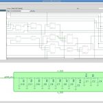
One of the surprises at DAC for ICScape was to be listed on Gary Smith’s list of companies to see. Surprised, since ICScape had never presented their products to him. They were listed under design debug. They don’t have a single product that really falls under that description, but rather a family of tools under the ICExplorer… Read More
I have been observing Fractal Technologiesexhibiting at DACyear after year, and every year they have demonstrated good value added features in their tools for SoC and IP development. This year at 52[SUP]nd[/SUP] DAC Fractal’s booth number is 1110. Earlier in this year Fractal had added a new ‘Cdiff’ feature in its flagship product… Read More
These days it’s common to expect large digital designs, analog blocks, custom IPs, glue logic, interfaces and interconnects all developed separately, perhaps by different vendors / teams, but integrated together in a single environment forming an SoC. The SoC can have multiple clock domains and can work in multiple modes of … Read More
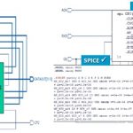
Spice view of a design, block or fragment of the design is probably the lowest level of functional description of a circuit in terms of transistors, resistors, capacitors, interconnect and so on, which in several ways acts as an ultimate proof of pudding for any semiconductor design before manufacturing. However, it’s generally… Read More
In a complex environment of semiconductor design where an SoC can have several millions of gates and multiple number of IPs at different levels of abstractions from different sources integrated together, it becomes really difficult to understand and debug the overall SoC design. Of course, along with the SoC integration, optimization… Read More
A semiconductor SoC design can have multiple components at different levels of abstractions from different sources and in different languages. While designing an SoC, IPs at different levels have to be integrated without losing the overall design goals. Of course, quality of an IP inside and outside of an SoC must be tested thoroughly.… Read More
In an environment of SoCs with tough targets of multiple functionalities, smallest size, lowest power and fastest performance to achieve within a limited design cycle window in order to meet the rigid time-to-market requirements, any day spent without success becomes very frustrating for a designer. Especially during tape-out… Read More
Debugging an IC design at the transistor, Gate and RTL levels is often necessary to meet timing requirements and understand analog or digital behavior, yet the process itself can be a tedious one, filled with manual steps, therefore making it an error-prone process. EDA tools have been created to help us graphically debug transistor,… Read More