You are currently viewing SemiWiki as a guest which gives you limited access to the site. To view blog comments and experience other SemiWiki features you must be a registered member. Registration is fast, simple, and absolutely free so please,
join our community today!
With the advent of large SoCs in semiconductor design space, verification of SoCs has become extremely challenging; no single approach works. And when the size of an SoC can grow to billions of gates, the traditional methods of testability of chips may no longer remain viable considering the needs of large ATPG, memory footprint,… Read More
3D-IC has a stack of dies connected and packaged together, and therefore needs new testing strategies other than testing a single die. It’s given that a single defective die can render the whole of 3D-IC unusable, so each die in the stack must be completely and perfectly tested before its entry into that stack. Looking at it from a … Read More
It’s a fact that new process nodes come with some amount of yield challenges. One way to find and eliminate silicon defects is through diagnosis-driven yield analysis (DDYA), which is the topic of a free seminar by Mentor Graphics in Fremont this Thursday, October 10 from 11:30am – 2pm (yes, lunch is included because Mentor… Read More
I am talking about the health of electronic and semiconductor design, which if made sound at RTL stage, can set it right for the rest of the design cycle for faster closure and also at lesser cost. Last week was the week of ITC(International Test Conference) for the Semiconductor and EDA community. I was looking forward to what ITC… Read More
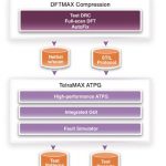
On my first job out of college as an IC design engineer I was surprised to discover that a major cost of chips was in the amount of time spent on the tester before being shipped. That is still true today, so how would you keep your tester time down, test coverage high and with a minimum number of pins when using multiple processors on a single… Read More
A Goldmine of Tester Databy Beth Martin on 07-10-2013 at 2:06 pmCategories: EDA
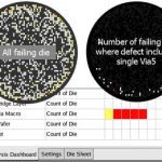
Yesterday at SEMICON West I attended an interesting talk about how to use the masses of die test data to improve silicon yield. The speaker was Dr. Martin Keim, from Mentor Graphics.
First of all, he pointed out that with advanced process nodes (45nm, 32nm, and 28nm), and new technologies like FinFETs, we get design-sensitive defects.… Read More
SEMICON West is next week, July 9-11 in San Francisco. If you haven’t signed up, and want to attend for free instead of $100,
1) Send an email to silicon_test@mentor.com with subject line “Semicon pass.”
2) Register for SEMICON West
3) After registering, download the SEMICON West mobile app and start building your schedule. Here… Read More
What: DAC lunch seminar (register here)
When: June 5, 2013, 11:30am – 1:30pm
Where: At DAC in lovely Austin, TX
Dr. Martin Keim of Mentor Graphics will present this overview of the new the IEEE P1687 standard, called IJTAG for ‘internal’ JTAG.
If you are involved in IC test*, you’ve probably heard about IJTAG. If you … Read More
One of the best things about being part of SemiWiki is the exposure to new technologies and the people behind them. SemiWiki now works with more than 35 companies and I get to spend time with each and every one of them. Much like I do, IROC Technologies works closely with the foundries and the top semiconductor companies so it was a pleasure… Read More
IJTAG for IP Test: a free seminarby Beth Martin on 03-14-2013 at 1:53 pmCategories: EDA, Siemens EDA
What: Better IP Test with IJTAG
When: 26 March, 2013, 10:30am-1:30pm
Where: Mentor Graphics, 46871 Bayside Parkway, Fremont, CA 94538
If you are involved in IC test*, you’ve probably heard about the IEEE P1687 standard, called IJTAG for ‘internal’ JTAG. IJTAG defines a standard for embedded IP that includes simple… Read More