You are currently viewing SemiWiki as a guest which gives you limited access to the site. To view blog comments and experience other SemiWiki features you must be a registered member. Registration is fast, simple, and absolutely free so please,
join our community today!
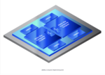
Artificial intelligence (AI) and machine learning (ML) are evolving at an extraordinary pace, powering advancements across industries. As models grow larger and more sophisticated, they require vast amounts of data to be processed in real-time. This demand puts pressure on the underlying hardware infrastructure, particularly… Read More
What looks like a modest market expansion strategy is all but modest.
Insights into the Semiconductor Industry and the Semiconductor Supply Chain.
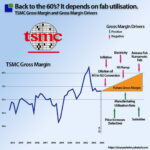
As usual, when TSMC reports, the Semiconductor industry gets a spray of insights that help understand what goes on in other areas of the industry. This time, TSMC gave more insight … Read More
The TSMC Technology Symposium provides a worldwide stage for TSMC to showcase its advanced technology impact and the extensive ecosystem that is part of the company’s vast reach. These events occur around the world and the schedule is winding down. TSMC covers many topics at its Technology Symposium, including industry-leading… Read More
My dog yawns every time I say Semiconductor or Semiconductor Supply Chain. Most clients say, “Yawn…. Don’t pontificate – pick the Nasdaq winners for us!”
If you follow along with me, you might gain some insights into what is happening in AI hardware. I will leave others to do the… Read More
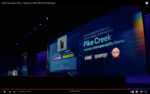
Intel recently made headlines when CEO Pat Gelsinger unveiled the world’s first UCIe interoperability test chip demo at Innovation 2023. The test chip built using advanced packaging technology is codenamed Pike Creek and is used to demonstrate interoperability across chiplets designed by Intel and Synopsys. More details … Read More
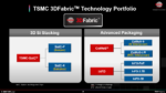
TSMC’s 3DFabric initiative was a big focus at the symposium, as it should be. I remember when TSMC first went public with CoWos the semiconductor ecosystem, including yours truly, let out a collective sigh wondering why TSMC is venturing into the comparatively low margin world of packaging. Now we know why and it is absolutely… Read More
Throughout its history, the ASIC industry has had its ups and downs. With feast and famine cycles, the ASIC business model is not for the faint of heart. Some companies tread boldly while others dread the cycles and stay away from this business model. Those who are consistently successful have to overcome many challenges thrown … Read More
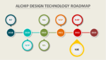
TSMC recently held their annual Technology Symposium in Santa Clara, CA. The presentations provide a comprehensive overview of their technology status and upcoming roadmap, covering all facets of the process technology and advanced packaging development. This article will summarize the highlights of the advanced packaging… Read More
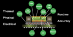
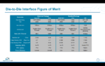
The topic of chiplets is getting a lot of attention these days. The chiplet movement has picked up more momentum since Moore’s law started slowing down as process technology approached 5nm. With the development cost of a monolithic SoC crossing the $500M and wafer yields of large die-based chips dropping steeply, the decision … Read More
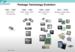
From DIP to Advanced, semiconductor packaging has become strategic
For ease of reading – I am going to be splitting this primer into two parts. First is the technical overview of everything. Next will be the company-specific writeups that follow over time – specifically Teradyne, Formfactor, Advantest, and Camtek
…
Read More