You are currently viewing SemiWiki as a guest which gives you limited access to the site. To view blog comments and experience other SemiWiki features you must be a registered member. Registration is fast, simple, and absolutely free so please,
join our community today!
Just prior to the opening of the 54[SUP]th[/SUP] Design Automation Conference, Mentor, a Siemens company, and PhoeniX Software issued a press release announcing a new integration between their tools to help designers of photonic ICs (PICs) to close the loop for manufacturing sign-off verification. This is a significant piece… Read More
After reading the Cadence blog post –“Dracula, Vampire, Assura, PVS: A Brief History” – Dr. Andrew Moore has written the below article where he helps readers get a sense as to what “the year of hell” was like, from one of the key individuals who lived it. Andrew also addresses and corrects some of the “urban legends”… Read More
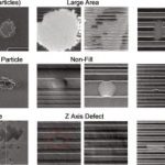
It seems like I have written a lot about SRAM lately. Let’s face it SRAM is important – it often represents large percentages of the area on SOC’s. As such, SRAM yield plays a major role in determining overall chip yields. SRAM is vulnerable to defect related failures, which unlike variation effects are not Gaussian in nature. Fabrication… Read More
I caught up with John Ferguson of Mentor Graphics this week to learn more about a recent announcement that TSMC has extended its collaboration with Mentor in the area of Fan-Out Wafer Level Processing (FOWLP).
In March of last year Mentor and TSMC announced that they were collaborating on a design and verification flow for TSMC’s… Read More
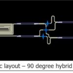
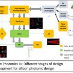
A few weeks back I wrote an article mentioning that Mentor Graphics has been quietly working on solutions for photonic integrated circuits (PICs) for some time now, while one of their competitors has recently established a photonics beachhead. One of the most common challenges for PIC designs is their curvilinear nature, thus… Read More
If you don’t get the tongue in cheek reference of the title, you probably don’t have children who liked to watch Disney movies. All four of my daughters loved Disney and so, I am forever shaped by the Wonderful World of Disney. In 2007 Disney adapted to the screen a novel called, ‘A Bridge to Terabithia’, in which two adolescents escape… Read More
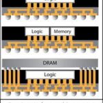
This year is shaping up to be an inflection point, when multi-die packaging technology will experience tremendous market growth. Advanced 2.5D/3D package offerings have been available for several years, utilizing a variety of technologies to serve as the package substrate, interposer material for embedding die micro-bump… Read More
Albert Einsteinhad said, “In the middle of difficulty lies opportunity”. In today’s world dominated by technology, or I must say internet which has initiated collaborative information sharing, “leading from the middle” is the new mantra of life.… Read More
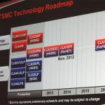
The technology for 10 nm is settled, but what about 7 nm and 5 nm? Those nodes will happen with silicon-based CMOS and 193nm immersion lithography, but exactly how is still being worked out. Right now, though, the focus is on getting 10 nm chips into high-volume production. TSMC and Intel both claim to be on track for high-volume manufacturing… Read More
The traditional system-on-chip (SoC) design process has fully qualified verification methods embodied in the form of process design kits (PDKs). Why is it that chip design companies and assembly houses have no IC/package co-design sign-off verification process?
Package die are often produced using multiple processes and… Read More