You are currently viewing SemiWiki as a guest which gives you limited access to the site. To view blog comments and experience other SemiWiki features you must be a registered member. Registration is fast, simple, and absolutely free so please,
join our community today!
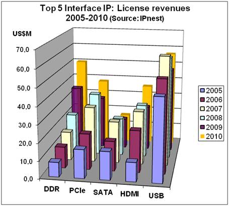
I have shared with you last year some strategic information released by Cadence in April about their IP strategy, more specifically about the launch of the DDR4 Controller IP. And try to understand Cadence strategy about Interface IP in general (USB, PCIe, SATA, DDRn, HDMI, MIPI…) and how Cadence is positioned in respect with their… Read More
Imera Virtual Fabricby Paul McLellan on 01-10-2012 at 6:00 amCategories: EDA
Virtual fabric sounds like something that would be good for making the emperor’s new clothes. I talked today to Les Spruiell of Imera to find out what it really is.
Anyone who has worked as either a designer or as an EDA engineer has had the problem of a customer who has a problem but can’t send you the design since it is (a)… Read More
During my annual holiday meal with one of my favorite EDA icons some rather bold predictions were made. On his side it was more of what he would LIKE to see happen, on my side it was more of what will HAVE to happen for the semiconductor ecosystem to thrive in the coming years.
Mike Gianfagna (Viva Italia!) spent 15+ years with RCA/GE Semiconductor… Read More
Every week I receive several webinar invitations, so the recent one from Cadence about Virtuoso Multi-Mode simulation caught my fancy because I had met with John Pierce at DAC and wanted to see what was new since then and see how they compared with Mentor and Synopsys tools.
John Pierce, Product Marketing Director
This webinar runs… Read More
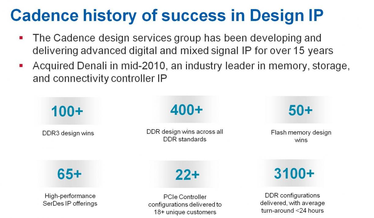
Denali acquisition by Cadence in May 2010, ChipIdea, Virage Logic, and nSys acquisitions by Synopsys in 2009, 2010 and 2011 (resp.) shows that IP market is consolidating… but new IP vendors are still emerging! So we need to know on which product the Interface IP market leader will tend to a dominant position, which new products… Read More
This was my first ARM TechCon, they cordially invited me as media, but it certainly was not what I expected. Making matters worse, I had literally just flown in from a very long weekend sailing in Mexico which was much more interesting and certainly made me much less tolerant of sales and marketing nonsense. My Uncle Jim lives on a sailboat… Read More
AnSem has been in the AMS design business since 1998 and uses a variety of commercial EDA tools along with internally developed tools and scripts to automate the process of analog design and technology porting. Their IC designers have completed some 40 AMS projects in diverse areas like:
- RF CMOS
- LNA, VCO, Mixers
- Synthesizers
- Low-IF/Zero-IF
…
Read More
I read about how Toumaz used the Analog Fast SPICE (AFS) tool from BDA and it sounded interesting so I setup a Skype call with Alan Wong in the UK last month to find out how they design their ultra low-power IC chips.
Interview
Q: Tell me about your IC design background.
A: I’ve been at Toumaz almost 8 years now and before that at Sony… Read More
The mobile devices market is simply exploding, with smartphones shipmentgoing up to the sky, tabletsemerging so fast that some people think it will replace PC (but this is still to be confirmed…). This lead mobile SoC designs to integrate increasingly more features, to support customer needs for more computing power and sophisticated… Read More
There are various rumors around about Cadence starting to close up stuff that has been open for a long time. Way back in the midst of time, as part of the acquisition of CCT, the Federal Trade Commission forced Cadence to open up LEF/DEF and allow interoperability of Cadence tools (actually only place and route) I believe for 10 years.… Read More