You are currently viewing SemiWiki as a guest which gives you limited access to the site. To view blog comments and experience other SemiWiki features you must be a registered member. Registration is fast, simple, and absolutely free so please,
join our community today!
We attended the Needham Growth Conference which is one of the first conferences of the year and in the quiet period before most companies reported so even though there was no “official” comment from most companies on the quarter, the surrounding commentary spoke volumes:
- The down cycle (and everyone admits its a cycle
…
Read More
It should come as no big surprise that Samsung will miss its Q4 numbers. The company pre announced that profits will be 10.8T KWON (about $9.7B ) versus the 13.2T KWON analysts had predicted, close to a 20% miss. This number is also down about 39% sequentially. Revenue at 59T KWON instead of expected 62.8T KWON and down about 10%. The… Read More
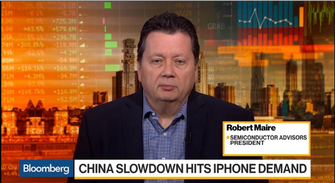
On the first day of trading in the new year Apple just announced, after the close, that revenues will be lower than previously expected coming in at $84B versus the expected range of $89B to $93B and analyst estimates of the current quarter at $91.5B. Ugly….. The blame was laid squarely on China as slowing sales and trade tensions… Read More
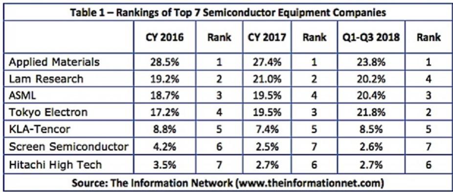
Semiconductor equipment vendor ranking, which didn’t change much between 2016 and 2017, is undergoing a makeover, as Lam Research, ASML, and Tokyo Electron (TEL) are switching places and top-ranked Applied Materials is getting closer to losing its number one ranking.
Since the 1990s, Applied Materials has been the market leader… Read More
The DOJ last week released a previously sealed indictment against UMC, Jinhua and three individuals for stealing Micron trade secrets. The indictment is very damning of UMC with very specific semiconductor technology files that were stolen by UMC related people then passed on to Jinhua through its joint development with UMC.… Read More
ASML reported EUR2.78B in revenues with EUR2.08B in systems. 58% was for memory. EUV was EUR513M with 5 systems. Importantly orders were for EUR2.20B in systems at 64% memory and 5 EUV tools. This was likely better than expectations given the overall industry weakness. EPS of EUR1.60 was more or less in line with expectations. Guidance… Read More
Given that the semiconductor industry is clearly in the midst of a down cycle (even though there are cycle deniers, also members of the flat earth society…), most investors and industry participants want to know the timing of the down cycle and the shape of the recovery as we want to know when its safe to buy the stocks again. … Read More
Applied Materials (AMAT) is batting clean up in a quarter that has not been pretty. Lately semi stocks seem to have been hit by not only stock specific issues but continued and increasing memory concerns coupled with more macro issues. On top of all this, China trade issues which have in the meantime taken a back burner to other issues… Read More
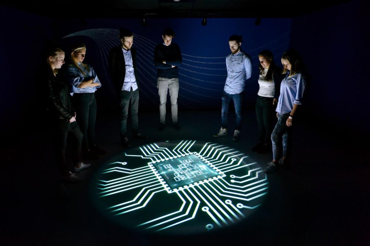
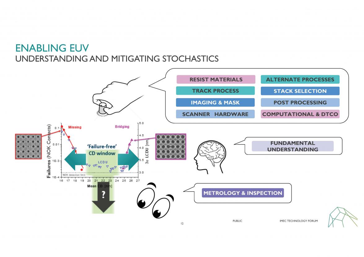
At SEMICON West I attended the imec technology forum, multiple Tech Spot presentations and conducted a number of interviews relevant to advanced lithography and EUV. In this article I will summarize what I learned plus make some comments on the outlook for EUV.… Read More
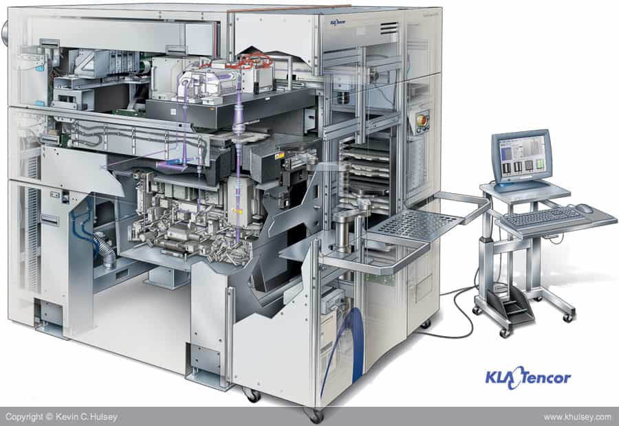
KLAC put up a great quarter coming in at revenues of $1.07B and EPS of $2.22. Guidance is for $1.03B to $1.1B with EPS of $2 to $2.32. Both reported and guided were at the high end of the range and above consensus. We had suggested in our preview notes that KLAC would be the least impacted of the big three (AMAT, LRCX & KLAC) semi equipment… Read More