You are currently viewing SemiWiki as a guest which gives you limited access to the site. To view blog comments and experience other SemiWiki features you must be a registered member. Registration is fast, simple, and absolutely free so please,
join our community today!
In the modern semiconductor ecosystem we are seeing rapid advancement in technology breaking past once perceived limits; 28nm, 20nm, 16-14nm, 10nm and we are foreseeing 7nm now. Double and multi-patterning are already being seen along with complex FinFET structures in transistors to gain the ultimate advantages in PPA from… Read More
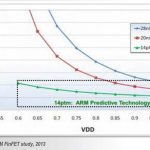
Since power has become a critical factor in semiconductor chip design, the stress is towards decreasing supply voltage to reduce power consumption. However, the threshold voltage to switch devices cannot go down beyond a certain limit and these results in an extremely narrow margin for noise between the two. And that gets further… Read More
IC designers have been running analysis tools for power, noise and reliability for many years now, so what is new when you start using FinFET transistors instead of planar transistors? Calvin Chow from ANSYS (Apache Design) presented on this topic earlier in the summer through a 33 minutewebinar that has been archived. There is… Read More
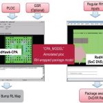
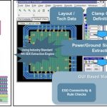
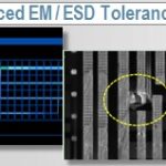
In this age of electronics, especially with so many different types of human held devices and more upcoming wearable devices, it’s utmost important to protect the massive circuitry inside those tiny parts in the devices from ESD related failures. The protection needs to happen at all stages – cells inside the chips, package… Read More
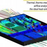
Last week my daughter was playing some games on my Google Nexus smartphone for a while when one of my friends called. When I picked up the phone, I couldn’t imagine it was so hot. There is no doubt; every electronic device today emits an order of magnitude higher heat than what it used to at most a decade ago. There is so much emphasis on … Read More
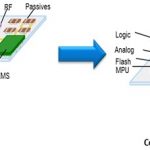
In today’s era of low power and high performance components, preferably on a single chip provides impetus to much larger electronic systems packaged into much smaller cases; smartphones are the immediate examples which encapsulate multiple functions other than the intended ones, viz. phone and data communication. As an example,… Read More
During my illustrious career one of the most useful axioms that I use just about everyday day is: “Understand what people say but also understand why they are saying it.” This certainly applies to press releases so let’s take a look at what Intel unleashed during #51DAC (in alphabetical order):
ANSYS And Intel Collaborate… Read More
My favorite method to learn about EDA tools at DAC is by listening to actual IC designers, so on June 3rd I heard Jacob Bakker from NXP talk about his experience with noise coupled analysis for advanced mixed-signal automotive ICs.… Read More
In the semiconductor industry, it feels great to hear about the process technology shrinking to lower nodes along with innovative transistor structures that offer major gains in PPA (Power, Performance and Area). However, it requires huge investment of capital, time and effort from foundries to conceptualize, prototype and… Read More
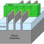
Although semiconductor manufacturing has taken off with FinFET based process technology which provides lucrative payoffs on performance improvement, power reduction and area saving in devices for high density and high performance SoC demand of modern era, apprehensions remain about its reliability due to reduced noise … Read More