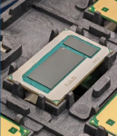
The semiconductor industry is entering a new era in which advanced packaging and chiplets-based architectures are becoming the primary drivers of system-level innovation. As traditional process-node scaling becomes increasingly complex and expensive, manufacturers are turning to heterogeneous integration, combining… Read More
Advanced Packaging Summit 2026, under the theme “Packaging the Future of AI – From Silicon to Photon,” will examine the evolution of packaging technologies in the AI era and their broader implications for the semiconductor industry. Featuring presentations by leading industry experts, the summit will explore market shifts… Read More
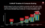
The rapid rise of artificial intelligence is fundamentally reshaping computing architectures. As AI models scale toward trillions of parameters, traditional approaches to performance improvement are no longer sufficient. Instead, the industry is entering a new era where system-level innovation, advanced packaging, … Read More
High-speed digital (HSD) design is one of the more exciting areas in EDA right now, with design practices, tools, and workflows evolving to keep pace with increasing design complexity. With the annual Chiplet Summit and DesignCon festivities right around the corner, we sat down with Keysight’s Hee-Soo Lee, HSD Segment Lead, … Read More
AI’s rapid expansion is reshaping semiconductor design. The compute and I/O needs of modern AI workloads have outgrown what traditional SoC scaling can deliver. As monolithic dies approach reticle limits, yields drop and costs rise, while analog and I/O circuits gain little from moving to advanced process nodes. To sustain … Read More
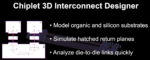
The semiconductor industry is rapidly moving beyond traditional 2D packaging, embracing technologies such as 3D integrated circuits (3D ICs) and 2.5D advanced packaging. These approaches combine heterogeneous chiplets, silicon interposers, and complex multi-layer routing to achieve higher performance and integration.… Read More
In a keynote delivered at this year’s Siemens EDA User2User event, CEO Mike Ellow presented a focused vision for the evolving role of electronic design automation (EDA) within the broader context of global technology shifts. The session covered Siemens EDA’s current trajectory, market strategy, and the changing landscape … Read More
Intel, long a leader in semiconductor manufacturing, is on a determined journey to reclaim its technological leadership in the industry. After facing significant challenges in recent years, the company is making a concerted effort to adapt and innovate, with a clear focus on AI-driven technologies, advanced packaging solutions,… Read More
Intel recently issued a press announcement that has significant implications for the future of semiconductors. The release announces Intel’s new glass substrate technology. The headline states: Glass substrates help overcome limitations of organic materials by enabling an order of magnitude improvement in design rules… Read More
From the multi-chip-modules (MCM) of yester years to today’s System-in-Package (SiP) implementations, things have progressed a lot in terms of package technology. The chiplet movement is not only a big beneficiary of today’s advanced package technologies but drives further advances in this technology area. While a chiplets-based… Read More