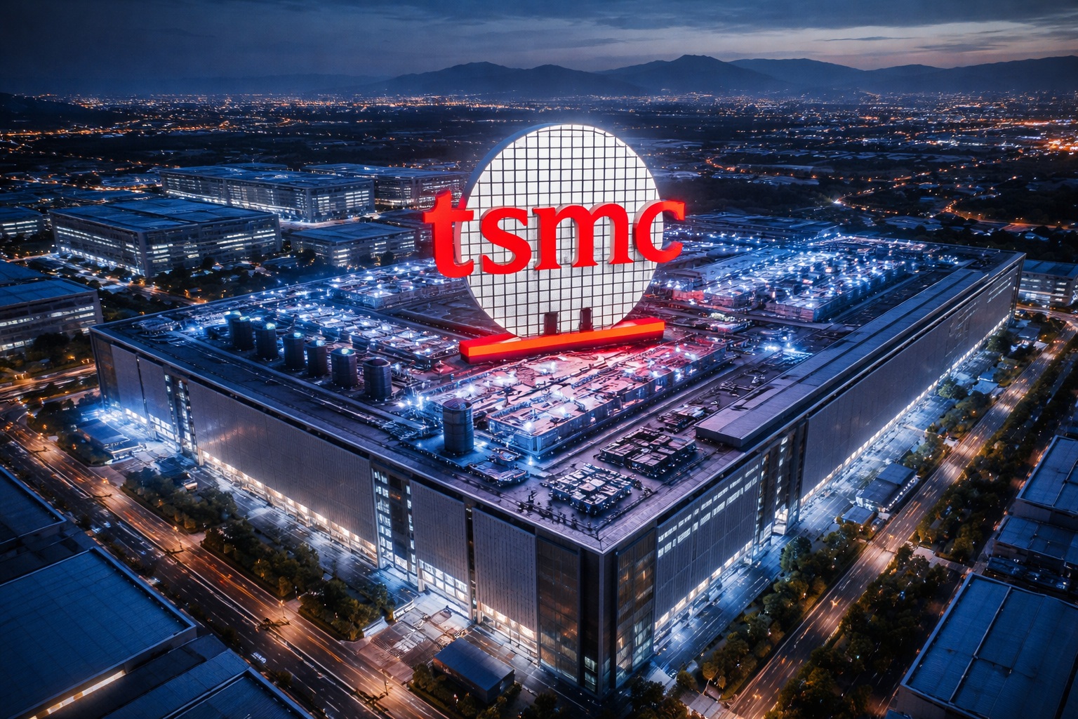


TSMC sits at the center of the global semiconductor ecosystem, and its transition to 2nm (TSMC N2) manufacturing has become one of the most closely watched developments in the technology industry. As demand for AI, HPC, and advanced mobile devices surges, TSMC’s ability to scale 2nm capacity will shape the trajectory of the entire semiconductor supply chain. The company’s expansion plans, production ramp, and capacity constraints illustrate both the opportunities and challenges of leading-edge semiconductor manufacturing.
TSMC began volume production of its N2 process in the fourth quarter of 2025, marking a major milestone in transistor scaling. This node introduces gate-all-around nanosheet transistors, which improve performance, reduce power consumption, and increase transistor density compared with previous 3nm technologies. Reports indicate that the N2 process delivers approximately a 10–15% performance improvement at the same power or a 25–30% power reduction at equivalent performance levels. These gains are crucial for AI accelerators and advanced mobile processors, both of which require more efficient compute density. This is design dependent of course.
Capacity ramp is the next major challenge. Early production is concentrated at new facilities in Taiwan, notably Fab 20 in Hsinchu and Fab 22 in Kaohsiung. Fab 20 alone is expected to deliver around 20,000–25,000 wafers per month during early production stages, reflecting the slow initial ramp typical for leading-edge nodes. As yields improve and additional lines come online, overall capacity is expected to expand rapidly.
Industry forecasts suggest that TSMC’s combined 2nm capacity could reach roughly 80,000 to 100,000 wafers per month by the end of 2026, with some estimates projecting up to 140,000 wafers monthly as more fabs scale production. These projections underscore the aggressive pace of expansion needed to meet customer demand.
However, demand appears to be outpacing supply. Reports indicate that TSMC’s initial 2nm capacity for 2026 has already been fully booked, with major customers such as Apple, AMD, Qualcomm, MediaTek, and Nvidia competing for allocation. In some cases, Apple alone is expected to consume more than half of early production capacity. This strong demand highlights the strategic importance of 2nm technology for next-generation devices.
This of course is completely nonsense to people like myself who actually know how wafer agreements work and understand CAPEX. It is still fun to read though, kind of like the tabloid headlines at the checkout counters.
The tight supply situation is reinforced by broader industry commentary. Recent reports indicate that TSMC is facing capacity constraints amid booming AI demand, with customers concerned about limited foundry availability through 2026. This bottleneck is pushing companies to secure long-term supply agreements and encouraging additional capital expenditure by TSMC to accelerate expansion.
To address these constraints, TSMC is investing heavily in advanced manufacturing. The company plans to allocate a significant portion of its capital expenditure—estimated between $52 billion and $56 billion for 2026—toward advanced process technologies, including 2nm and beyond. This investment supports new fabs, equipment upgrades, and advanced packaging capacity, all of which are required to scale 2nm production efficiently.
Longer-term projections indicate even larger capacity growth. Some industry estimates suggest TSMC could exceed 100,000 wafers per month of 2nm production by late 2026 and potentially reach around 200,000 wafers per month by 2028 as additional facilities come online, including potential U.S. manufacturing. Such expansion reflects the expectation that 2nm will quickly become the dominant node for high-performance computing and AI workloads.
Despite these ambitious plans, scaling 2nm capacity is not straightforward. Leading-edge fabs require massive infrastructure investments, specialized equipment, and advanced packaging ecosystems. Yield ramp challenges, power requirements, and supply chain constraints for critical components all complicate the process. Moreover, the shift to gate-all-around transistors increases manufacturing complexity, requiring new process steps and tighter tolerances.
Bottom line: TSMC’s 2nm capacity expansion represents both a technological breakthrough and a logistical challenge. While the company has successfully entered volume production and plans aggressive scaling, demand from AI and high-performance computing markets is likely to keep supply tight in the near term. The pace at which TSMC expands its 2nm capacity will influence semiconductor innovation, competitive dynamics among chip designers, and the broader global technology ecosystem.
Also Read:
TSMC Technology Symposium 2026: Advancing the Future of Semiconductor Innovation
Global 2nm Supply Crunch: TSMC Leads as Intel 18A, Samsung, and Rapidus Race to Compete
TSMC Process Simplification for Advanced Nodes
Share this post via:


Comments
There are no comments yet.
You must register or log in to view/post comments.