


When Intel entered the foundry business with IDM 2.0 I was impressed. Yes, Intel had tried the foundry business before but this time they changed the face of the company with IDM 2.0 and went “all-in” so to speak. The progress has been impressive and today I think Intel is well positioned to capture the NOT TSMC business by providing a trusted alternative to the TSMC leading edge business. The one trillion dollar questions is: Will Intel take business away from TSMC on a competitive basis? I certainly hope so, for the greater good of the semiconductor industry.
On the most recent TSMC investor call, which is the first call with C.C. Wei as Chairman and CEO, TSMC branded their foundry strategy as Foundry 2.0. It is not a change of strategy, it is a new branding based on what TMSC has been successfully doing for years now, adding additional products and services to keep customers engaged. 3D IC packaging is a clear example but certainly not the only one. The Foundry 2.0 brand is well earned and is clearly targeted at Intel IDM 2.0 which I think is funny and a great example of CC Wei’s sharp wit.
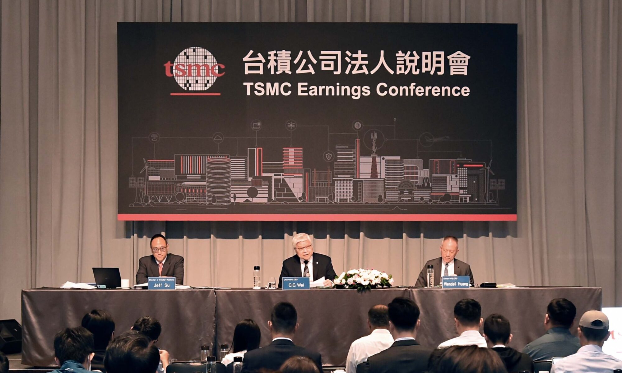
I thought for sure that Intel 18A would be the breakout foundry node for Intel but according to the TSMC investor call, that is not the case. TSMC N3 was a runaway hit with 100% of the major design wins. Even Intel used TSMC N3. I hadn’t seen anything like this since TSMC 28nm which was on allocation as a result of being the only viable 28nm HKMG node out of the gate. History repeated itself with N3 due to the delay of 3nm alternatives. This made the TSMC ecosystem the strongest I have ever witnessed with both the domination of N3 and TSMC’s rapidly expanding packaging success. I had originally thought that some customers would stick with N3 until the second generation of N2 appeared but I was wrong. On yesterday’s investor call:
CC Wei: We expect the number of the new tape-outs for 2-nanometer technologies in its first two years to be higher than both 3-nanometer and 5-nanometer in their first two years. N2 will deliver full load performance and power benefit, with 10 to 15 speed improvement at the same power, or 25% to 30% power improvement at the same speed, and more than 15% chip density increase as compared with the N3E.
CC had mentioned this before but I can now confirm this based on my hallway discussions inside the ecosystem at recent conferences: N2 designs are in progress and will start taping out towards the end of this year.
I really don’t think the TSMC ecosystem gets enough credit, especially after the overwhelming success of N3, but the N2 node is a force in itself:
CC Wei: N2 technology development is progressing well, with device performance and yield on track or ahead of plan. N2 is on track for volume production in 2025 with a ramp profile similar to N3. With our strategy of continuous enhancement, we also introduce N2P as an extension of our N2 family. N2P features a further 5% performance at the same power or 5% to 10% power benefit at the same speed on top of N2. N2P will support both smartphone and HPC applications, and volume production is scheduled for the second half of 2026. We also introduce A16 as our next nanosheet-based technology, featuring Super Power Rail, or SPR, as a separate offering.
And, of course, the TSMC freight train continues:
CC Wei: TSMC’s SPR is an innovative, best-in-class backside power delivery solution that is forcing the industry to incorporate another backside contact scheme to preserve gate density and device with flexibility. Compared with N2P, A16 provides a further 8% to 10% speed improvement at the same power, or 15% to 20% power improvement at the same speed, and additional 7% to 10% chip density gain. A16 is best suited for specific HPC products with complex signal routes and dense power delivery network. Volume production is scheduled for the second half of 2026. We believe N2, N2P, A16, and its derivative will further extend our technology leadership position and enable TSMC to capture the growth opportunities way into the future.
Congratulations to TSMC on their continued success, it is well deserved. I also congratulate the Intel Foundry team for making a difference and I hope the 14A foundry node will give the industry a trusted alternative to TSMC out of the starting gate. In my opinion, had it not been for Intel and of course CC Wei’s leadership and response to Intel’s challenge, we as an industry would not be quickly approaching the one trillion dollar revenue mark. Say what you want about Nvidia, but as Jensen Huang openly admits, TSMC and the foundry business is the real hero of the semiconductor industry, absolutely.
Also Read:
Has ASML Reached the Great Wall of China
The China Syndrome- The Meltdown Starts- Trump Trounces Taiwan- Chips Clipped
SEMICON West- Jubilant huge crowds- HBM & AI everywhere – CHIPS Act & IMEC
Share this post via:


Musk’s Orbital Compute Vision: TERAFAB and the End of the Terrestrial Data Center