The TSMC Technical Symposium is today so I wanted to give you a brief summary of what was presented. Tom Dillinger will do a more technical review as he has done in the past. I don’t want to steal his thunder but here is what I think are the key takeaways. First a brief history lesson.
The history of TSMC Technology Development with 12 key milstones:
In 1987 TSMC was founded with the creation of the PurePlay business model.
In 1999 TSMC was the first foundry to offer 0.18 micron copper technology.
2001 brought the first foundry reference design flow. I participated in this with multiple EDA and IP vendors and I can tell you first hand that TSMC spent a huge amount of money creating the massive EDA and IP ecosystem we enjoy today.
In 2011 TSMC brought HKMG 28nm to the fabless ecosystem. Other foundries faltered at 28nm so this was a record breaking node for TSMC.
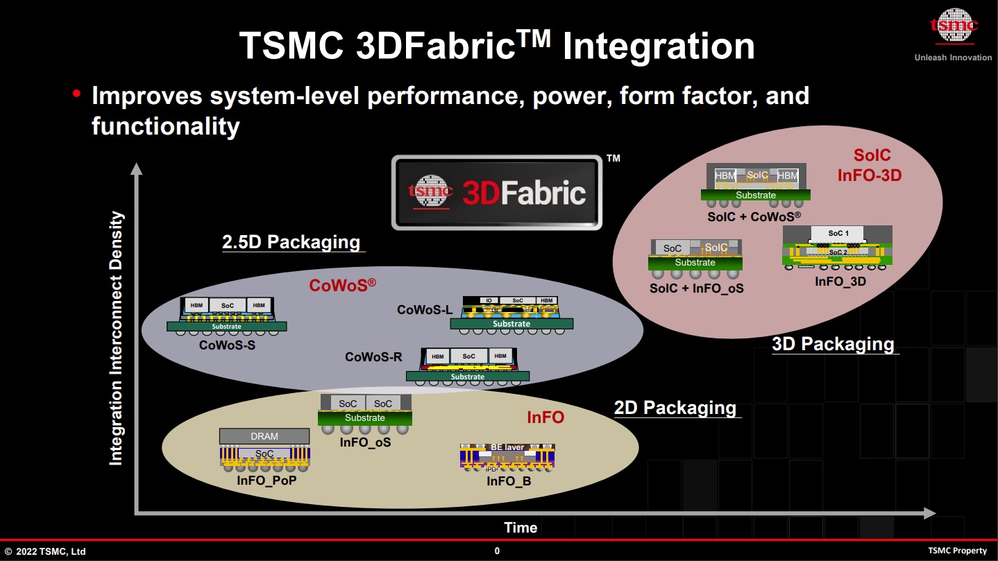
2012 brought CoWos, the first heterogenous 3DIC test vehicle.
In 2014 TSMC delivered the first fully functional FinFET networking processor which began the FinFET era that TSMC dominates today.
In 2015 TSMC qualified InFo, the advanced 3DIC packaging technology.
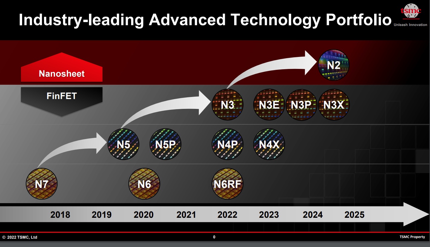
In 2018 TSMC delivered the most advanced logic technology (N7) available to all.
In 2020 TSMC lead the industry with N5 EUV based logic technology.
In 2021 TSMC launched N4P, N4X, and N6RF.
In 2022 TSMC will launch what will be the most advanced N3 process nodes covering a wide range of vertical markets. N3 will also break the record for tapeouts in a 5 year period, my opinion.
And last but not least, in 2022 TSMC announced the next generation process technology for the masses (N2).
Takeaway #1
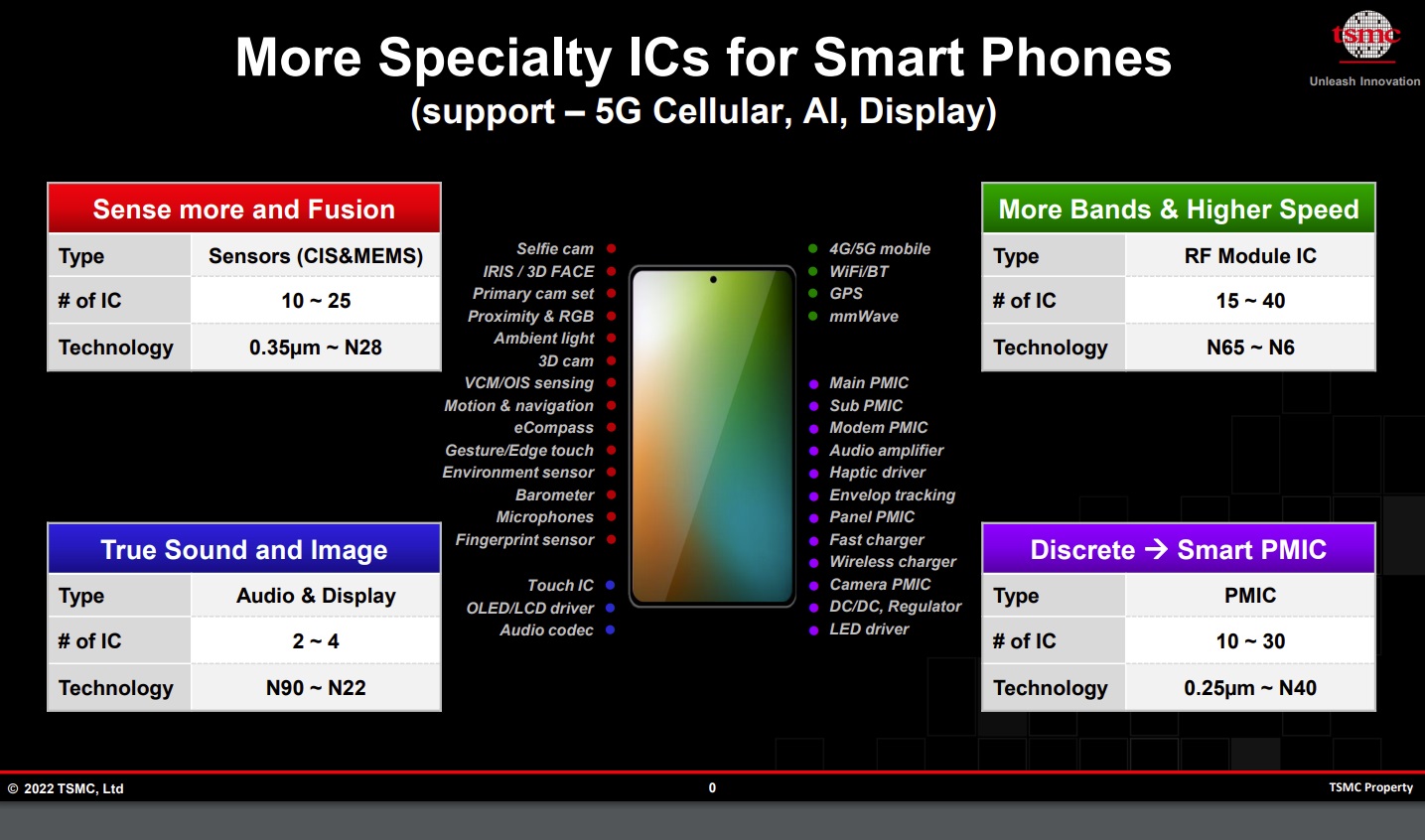
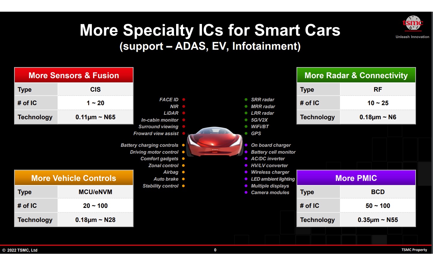
TSMC will continue to invest in mature node and specialty technologies with a 1.5x capacity expansion from 2021 to 2025 which includes Fabs F14P8 (Tianan), F16 P1B (Nanjing), F22 P2 (Kaohsiung) and fab F23 P1 (Kumamoto Japan).
TSMC also announced an Integrated Specialty Technology Platform for NVM, HV, Sensor, PMIC, ULP/ULL, analog, and RF technology. Tom Dillinger will go into more detail here.
Takeaway #2
TSMC will continue scaling N3. N3 is on track for HVM in 2H 2022. N3E follows in 2H 2023 with improved performance/power and low process complexity for both mobile and HPC applications.
N3E PPA versus N5 comes in at 18% speed at same power or 34% power reduction at same speed, and a 1.6x logic density increase.
More importantly, TSMC announced FinFlex: Ultimate Design Flexibility for N3. TSMC just published a blog on FinFlex with more detail. Tom Dillinger will also have his say on this so stay tuned. Bottom line: you can change fin configurations to further optimize designs for area, speed, and power.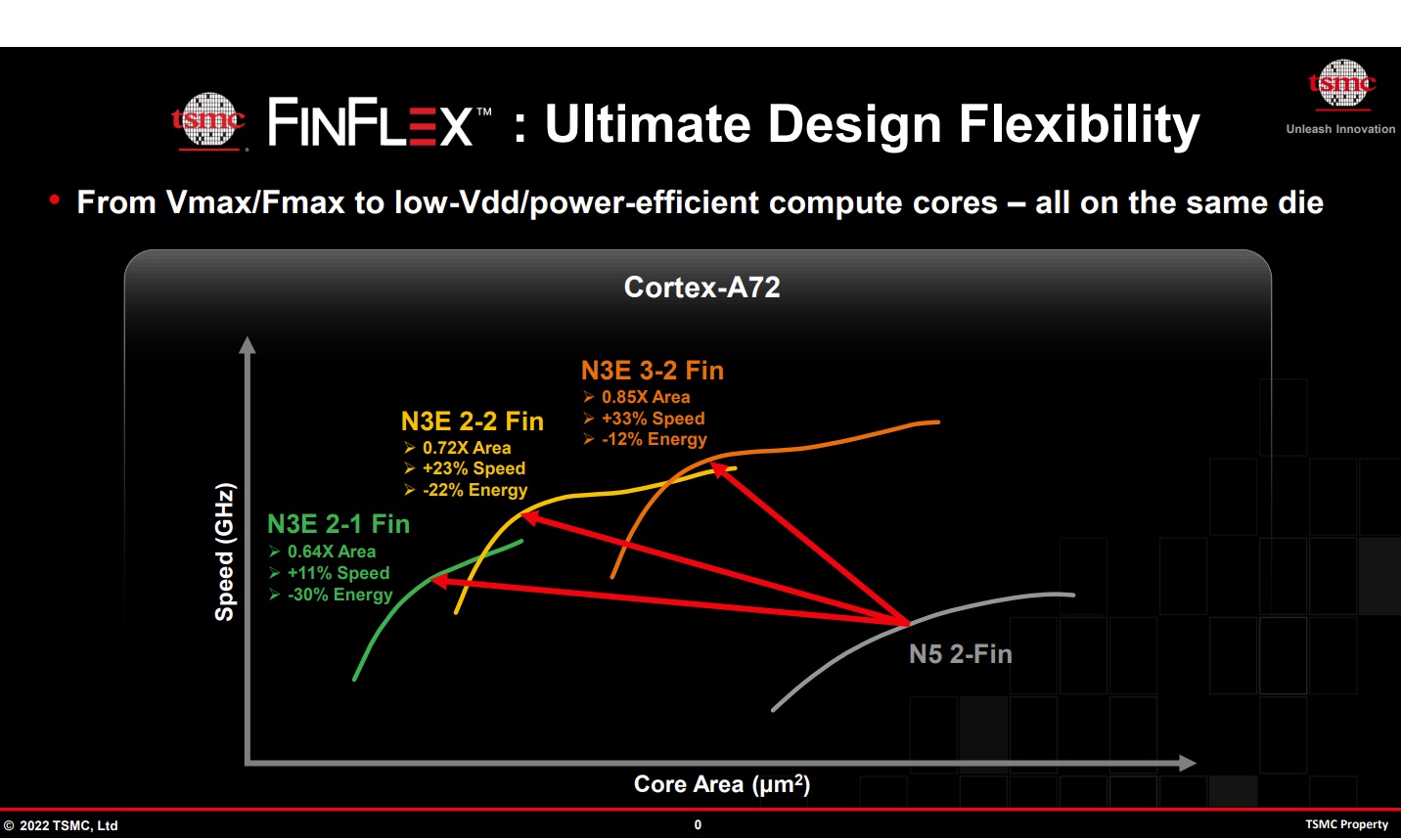
Takeaway #3
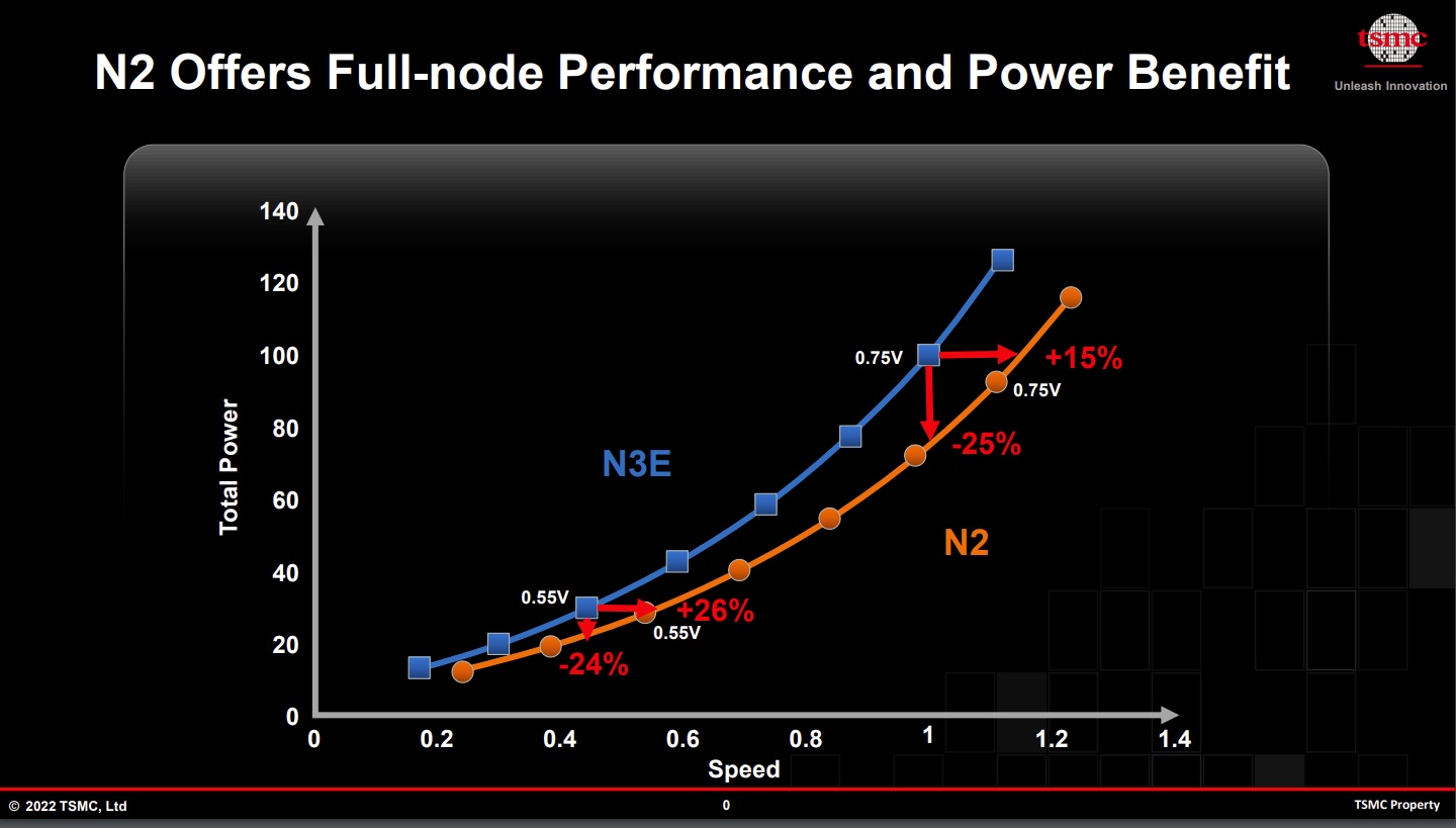
TSMC will use nanosheet transistors for N2. Not a huge surprise since Intel and Samsung have already made announcements but there is much more here than meets the eye. N2 PPA vs N3E is expected to be a 15% speed improvement at the same power or 25-30% power improvement at the same speed, and > 1.1x density. N2 is expected in 2025.
TSMC also discussed device architecture futures which included Nanosheet, CFET, 2D TMD, and CNT. We will be writing more about this later.
Bottom line: One thing we must all remember is that there is a distinct difference between a PurePlay and an IDM foundry. TSMC must produce the most cost effective, wide ranging process technologies with a fully supported ecosystem for hundreds of products. IDM foundries can pick and choose what is important and don’t have to worry about wafer margins. Semiconductor insiders know this but the media does not so expect continued misinformation in the coming days, absolutely.
So many more things were presented. If you have questions post them in the comments section and I will get the answers for you, absolutely.
Also Read:
Inverse Lithography Technology – A Status Update from TSMC
TSMC N3 will be a Record Setting Node!
Share this post via:


Comments
18 Replies to “Three Key Takeaways from the 2022 TSMC Technical Symposium!”
You must register or log in to view/post comments.