Summary
As a result of extensive focus on the development of workfunction metal (WFM) deposition, lithography, and removal, both FinFET and gate-all-around (GAA) devices will offer a wide range of Vt levels for advanced process nodes below 7nm.
Introduction
Cell library and IP designers rely on the availability of nFET and pFET devices with a range of threshold voltages (Vt). Optimization algorithms used in physical synthesis flows evaluate the power, performance, and area (PPA) of both cell “drive strength” (e.g., 1X, 2X, 4X-sized devices) and cell “Vt levels” (e.g., HVT, SVT, LVT) when selecting a specific instance to address timing, noise, and power constraints. For example, a typical power optimization decision is to replace a cell instance with a higher Vt variant to reduce leakage power, if the timing path analysis margins allow (after detailed physical implementation). The additional design constraints for multi-Vt cell library use are easily managed: (1) the device Vt active area must meet (minimum) lithography area requirements, and (2) the percentage of low Vt cells used should be small, to keep leakage currents in check.
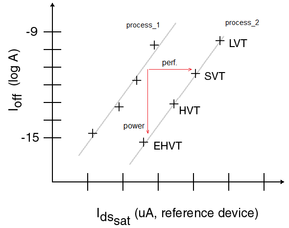
A common representation to illustrate the device Vt offerings in a particular process is to provide an I_on versus I_off characterization curve, as shown in the figure below.
Although it doesn’t reflect the process interconnect scaling options, this curve is also commonly used as a means of comparing different processes, as depicted in the figure. A horizontal line shows the unloaded, I_on based performance gains achievable. The vertical line illustrates the iso-performance leakage I_off power reduction between processes, for a reference-sized device in each. Note that these lines are typically drawn without aligning to specific (nominal) Vt devices in the two process nodes.
The I_on versus I_off curve does not really represent the statistical variation in the process device Vt values. A common model for representing this data is the Pelgrom equation. [1] The standard deviation of (measured) device Vt data is plotted against (1 / sqrt(Weff * Lgate)):
(sigma_Vt)**2 = (A**2) / 2 * Weff * Lgate
where A is a “fitting” constant for the process
Essentially , as the square root of the channel area of the device is increased, the sigma-Vt decreases. (Consider N devices in parallel with independent Vt variation – the Vt mean of the total will be the mean of the Vt distribution, while the effective standard deviation is reduced.) The Pelgrom plot for the technology is an indication of the achievable statistical process control – more on Vt variation shortly.
For planar CMOS technologies, Vt variants from the baseline device were fabricated using a (low impurity dose) implant into the channel region. A rather straightforward Vt implant mask lithography step was used to open areas in the mask photoresist for the implant. For an implant equivalent to the background substrate/well impurity type, the device Vt would be increased. The introduction of an implant step modifying the background concentration would increase the Vt variation, as well.
With the introduction of FinFET channel devices, the precision and control of implant-based Vt adjusts became extremely difficult. The alternative pursued for these advanced (high-K gate oxide, metal gate) process nodes is to utilize various gate materials, each with a different metal-to-oxide workfunction contact potential.
Vt offerings for advanced nodes
As device scaling continues, workfunction metal (WFM) engineering for Vt variants is faced with multiple challenges. A presentation at the recent VLSI 2020 Symposium by TSMC elaborated upon these challenges, and highlighted a significant process enhancement to extent multi-Vt options for nodes below 7nm. [2]
The two principal factors that exacerbate the fabrication of device Vt’s at these nodes are shown in the figures below, from the TSMC presentation.
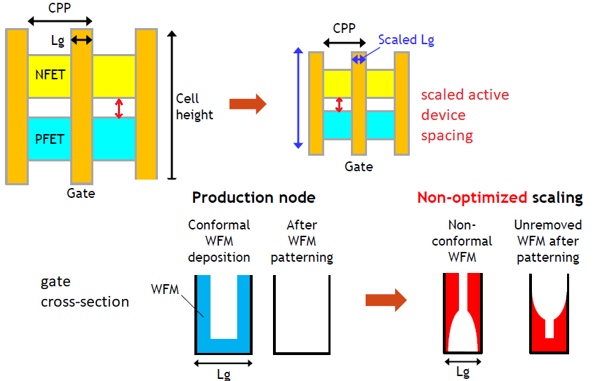
- The scaling of the device gate length (shown in cross-section in the figure) requires that the WFM deposition into the trench be conformal in thickness, and be thoroughly removed from unwanted areas.
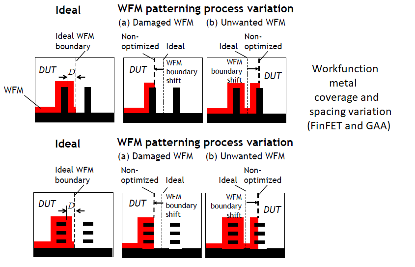
- Overall process scaling requires aggressive reduction in the nFET to pFET active area spacing. Lithographic misalignment and/or non-optimum WFM patterning may result in poor device characteristics – the figure above illustrates incomplete WFM coverage of the (fin and/or GAA) device.
Parenthetically, another concern with the transition to GAA device fabrication is the requirement to provide a conformal WFM layer on all side of each (horizontal) nanosheet, without “closing off” the gap between sheets.
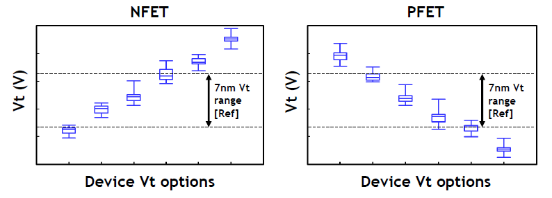
The TSMC presentation emphasized the diverse requirements of HPC, AI, 5G comm., and mobile markets, which have different top priorities among the PPA tradeoffs. As a result, despite the scaling challenges listed above, the demand for multi-Vt cell libraries and PPA optimization approaches remains strong. TSMC presented extremely compelling results of their WFM fabrication engineering focus. The figure below illustrates that TSMC has demonstrated a range of Vt offerings for sub-7nm nodes, wider than 7nm. TSMC announced an overall target Vt range exceeding 250mV. (Wow.)
In addition to the multi-Vt data, TSMC provided corresponding analysis results for the Vt variation (Pelgrom plot) and the time-dependent device breakdown (TDDB) reliability data – see the figures below.
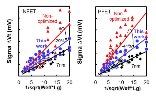
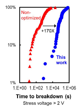
The sigma-Vt Pelgrom coefficient is improved with the new WFM processing, approaching the 7nm node results. The TDDB lifetime is also improved over the original WFM steps.
The markets driving the relentless progression to advanced process nodes have disparate performance, power, and area goals. The utilization of multi-Vt device and cell library options has become an integral design implementation approach. The innovative process development work at TSMC continues this design enablement feature, even extending this capability over the 7nm node – that’s pretty amazing.
For more information on TSMC’s advanced process nodes, please follow this link.
-chipguy
References
[1] ] M. J. M. Pelgrom, C. J. Duinmaijer, and A. P. G. Welbers, “Matching properties of MOS transistors”, IEEE J. Solid-State Circuits, vol. 24, no. 5, pp. 1433–1440, Oct. 1989.
[2] Chang, Vincent S., et al., “Enabling Multiple-Vt Device Scaling for CMOS Technology beyond 7nm Node”, VLSI Symposium 2020, Paper TC1.1.
Images supplied by the VLSI Symposium on Technology & Circuits 2020.
Share this post via:



Comments
There are no comments yet.
You must register or log in to view/post comments.