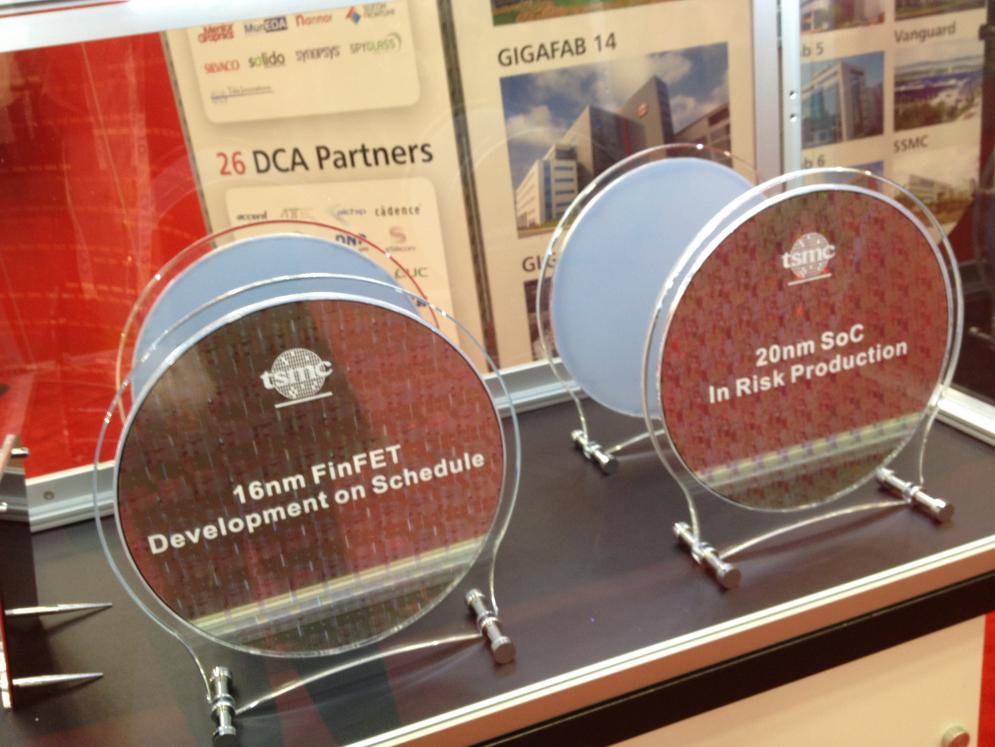
 The TSMC Open Innovation Platform® (OIP) Ecosystem Forum brings TSMC’s design ecosystem member companies together to share with our customers real-case solutions for customers’ design challenges and success stories of best practice in TSMC’s design ecosystem.
More than 90% of the attendees last year said “this forum helped them better understand the components of TSMC’s Open Innovation Platform” and “they found it effective to hear directly from TSMC OIP member companies.”
This year, the forum will feature a day-long conference starting with executive keynotes from TSMCin the morning plenary session to outline future design challenges and roadmaps, as well as discuss a recent collaboration announcement, 30 selected technical papersfrom TSMC’s EDA, IP, Design Center Alliance and Value Chain Aggregator member companies, and an Ecosystem Pavilion featuring up to 80 member companies showcasing their products and services.
Date: Tuesday, October 1st, 2013
Place: San Jose Convention Center
Attendees will learn about:
- Design challenges in 16nm FinFET, 20nm, and 28nm
- Successful, real-life applications of design technologies and IP
- Ecosystem specific implementations in TSMC reference flows
- New innovations for next generation product designs
In addition, attendees will hear directly from our design ecosystem member companies talk exclusively about design solutions using TSMC technologies, and enjoy valuable opportunities for peer networking with near 1,000 of industry experts and end users.
TSMC Open Innovation Platform Ecosystem Forum is an “invitation-only” event: : please register in order to attend. We look forward to seeing you at the 2013 Open Innovation Platform Ecosystem Forum.
Established in 1987, TSMC is the world’s first dedicated semiconductor foundry. As the founder and a leader of the Dedicated IC Foundry segment, TSMC has built its reputation by offering advanced and “More-than-Moore” wafer production processes and unparalleled manufacturing efficiency. From its inception, TSMC has consistently offered the foundry segment’s leading technologies and TSMC COMPATIBLE® design services.
TSMC has consistently experienced strong growth by building solid partnerships with its customers, large and small. IC suppliers from around the world trust TSMC with their manufacturing needs, thanks to its unique integration of cutting-edge process technologies, pioneering design services, manufacturing productivity and product quality.
The company’s total managed capacity reached 15.1 million eight-inch equivalent wafers in 2012. TSMC operates three advanced 12-inch wafer fabs, four eight-inch wafer fabs, and one six-inch wafer fab in Taiwan. TSMC also manages two eight-inch fabs at wholly owned subsidiaries: WaferTech in the United States and TSMC China Company Limited. TSMC also obtains eight-inch wafer capacity from other companies in which the Company has an equity interest.
lang: en_US
Share this post via:


Comments
There are no comments yet.
You must register or log in to view/post comments.