18 months ago Renesas announced they were prototyping their SG-MONOS eFlash on 28nm, and at the time we said it would be a couple of years before actual product. Yesterday, Renesas revealed their partner in this effort is TSMC – no surprise – and hinted things are moving, with better performance than expected but on a longer qualification timeline than anticipated. Continue reading “Pushing automotive-grade embedded flash to 28nm”
TSMC Fab 12 is a Pokemon Go Stop!
It only seems fitting that Fab 12 is a PokeStop since TSMC stands to make a lot of money from the augmented reality gaming craze that is sweeping the world. Unfortunately, most of the press I have read about Pokemon Go has been negative but that is the new “negative media” world we live in. As a player myself (level 25) and a semiconductor professional (level 32) let me share my experience, observations, and opinions on Pokemon Go and augmented reality as the next semiconductor driver.
I downloaded Pokemon Go on July 10[SUP]th[/SUP] at the urging of my nephew. After suffering years of Pokemon cartoons, trading cards, posters, stuffed animals, and even Halloween costumes at the hands of my four children it seemed like the right thing to do. It was immediately a good fit for me since it involves three of my favorite things: Walking (I walk 20+ miles a week so I can eat with impunity), semiconductor technology, and the opportunity to beat my nephew at a video game.
One thing I can tell you is that Pokemon Go absolutely consumes my iPhone 6 as you will notice by the warmth and short lived battery life (2-3 PokeHours). It has also more than doubled my data usage which is subjective of course since I generally use less than 1GB of data per month. While most of the program is local to the smartphone there must be a serious cloud infrastructure behind it with millions of people playing around the world. So yes, AR is a semiconductor driver and this is just the tip of the iceberg.
Pokemon Go is a very strategic game that gets deeper with every new release so I do not see this as an Angry Birds or Candy Crush type of fad. Pokemon tapped into the nostalgic side of former Pokemon trainers and their parents plus the nerd market segment on a whole. It also shows that augmented reality games have serious location based business applications. For example, you can submit a request to make your business a PokeStop or a coveted PokeGym and my wife and I even got a 15% PokeDiscount on a meal.
If you have Pokemon questions you can post them in the comments section. Since my nephew is literally a Pokemon encyclopedia my learning curve was rather short. I also have the benefit of living near a park with a 1km track and 20+ PokeStops and since I work mostly from home I have much more time on my hands than the typical Silicon Valley gridlocked commuter.
With the overwhelming success of Pokemon Go I expect many more augmented reality games to follow. How about Trivial Pursuit? I also expect a surge in smartphone purchases which of course will keep TSMC and the fabless semiconductor ecosystem growing, absolutely.
On a side note, I was in Taiwan during the Pokemon Go launch last month. I had already been playing so my experience level was very high in comparison and my PokeMonsters were on steroids so I owned the Hsinchu PokeGyms. There were swarms of people playing this game and when they finally figured out it was me that was destroying them I got the rock star treatment. I did make a kid cry when one of my PokeMonsters destroyed six of his but that is all part of PokeLife.
Another benefit of Pokemon Go, besides the extra calories I get to eat, is that I walk different routes and discover new things. This little zen retreat is a PokeGym two blocks from the Hotel Royal in Hsinchu. I have been staying at the Royal for close to 20 years and I never knew this existed. You can also go on PokeBikeRides but you have to go slow (5mph) to get mileage credit. PokeDriving however is a very bad idea but I did see quite a bit of it in Hsinchu which made being a pedestrian even more dangerous than it already is.
Apple will NEVER use Intel Custom Foundry!
The media already has Apple and Intel in talks to make the A11 SoC in 2018 as a result of the recent Intel/ARM IP licensing deal. This is probably one of the funnier media bumbles I have read in a while so let’s talk about it in a little more detail.
“According to Nikkei Asian Review, Intel is now perfectly poised to give TSMC a good run for its money in as little as two years because any Apple chips after the A10/A11 should be fabricated by Intel.”
First a little bit of history: As we wrote in “Mobile Unleashed” Chapter 7, Intel had the opportunity to make Apple’s SoCs from the very start but Intel again could not see the forest for the trees:
“According to ex-CEO Paul Otellini, Intel had been in discussions about a mobile chip for Apple before the original iPhone design. The cloak of secrecy on the iPhone gave Intel little to go on, and they were skeptical of Apple’s volume projections. “There was a chip [Apple was] interested in that they wanted to pay a certain price for and not a nickel more, and that price was below our forecasted cost. I couldn’t see it,” said Otellini. Intel passed.”
The rumors of Intel making SoCs for Apple have persisted and will continue to do so no matter how ridiculous it is. The good news is that I have won many lunch bets against Intel making Apple SoCs and will continue to do so, absolutely.
The latest rumor comes from the Intel Developer’s Forum (IDF). IDF is an Intel sponsored conference to created to promote Intel and products based on Intel technology (the first IDF was in 1997). The last IDF I attended was the launch of Intel’s 14nm product in 2014 where Intel CEO (Brian Krzanich) told us that 14nm was yielding on schedule only to recant at the next investor’s call. Apparently you can say things at IDF that you can’t say to Wall Street but I digress…
Also read: Intel Comes Clean on 14nm Yield!
This year’s IDF was again in San Francisco and now that the dust has settled there were two big revelations in regards to the manufacturing of semiconductors:
[LIST=1]
The ARM announcement is being overblown and the EUV announcement is being underblown so the Intel PR group is doing a great job.
Background:Intel has officially been in the foundry business since 2010 but has yet to get significant traction. At 22nm, Achronix and Netronome are lead customers with very low volumes. At 14nm, Altera and Spreadtrum are Intel foundry customers but we have yet to see silicon. Meanwhile the rest of the SoC and FPGA industry has been in 14nm/16nm HVM for more than a year.
Intel licensing the ARM IP for 10nm foundry business is wishful thinking at best. First, the IP that Intel licensed is the ARM standard cell and SRAM libraries, the building blocks of SoCs. Second, the big SoC vendors make their own standard cell and SRAM libraries and have already taped-out their 10nm designs and will be in HVM mid 2017, about the same time Intel 10nm will be ready to get STARTED with the new ARM IP.
LG is the announced first Intel 10nm customer which makes sense. LG does not have the volume to work with TSMC 10nm as an early adopter, LG competes directly with Samsung, and GlobalFoundries is skipping 10nm so what foundry choice did they really have? Besides, the majority of LG phones use SoCs from QCOM and MTK so this really is a low risk business proposition.
Bottom line: This announcement is a big fat nothing burger with cheese…
The “no EUV at 7nm” announcement was much more meaningful. At the semiconductor conferences earlier this year Intel stated very clearly that they would use EUV at 7nm while TSMC moved forward with a non EUV 7nm (TSMC will start 7nm production in 1H 2018 and hit serious HVM in 2H 2018 with the iPhone 8). So TSMC was RIGHT and Intel was WRONG about EUV. This is not a big technical change but Intel 7nm will be even more expensive since EUV is a significant cost reduction.
Yes, Intel will argue that their 10nm and 7nm are better than the foundries (TSMC and Samsung) but that will have to be proven at the chip level which is based on PPAC (power, performance, area, AND cost). The foundries have beaten Intel at every node based on SoC PPAC and I do not expect that to change at 10nm or 7nm. If you disagree I will cover all lunch bets.
Also read:If an Intel 10nm transistor fell in the ARM forest
MediaTek is on the Move with TSMC!
MediaTek (MTK) recently made the news for announcing their first leading edge SoC (Helio X30), a 32% increase in quarter over quarter sales, and an expected 30% increase for the year. Both of which deserve a closer look as we move into the second half of 2016 which should be very strong for MTK TSMC, and the fabless semiconductor ecosystem.
First a little bit of history: MTK was originally part of pure-play foundry UMC making chips for the consumer electronics market but was spun out in 1997 and taken public on the Taiwan Stock Exchange in 2001. MKT started out making chips for DVD players, TV, and early mobile phones. They expanded into smartphones and tablets and today are the number two SoC company, QCOM being number one. QCOM dominates the high end SoCs/smartphones while MKT is known for mid to low end products.
Up to 2009, MTK’s success was in 2G until they launched a wide range of chips for 3G moving up to 40nm chips in 2012 (QCOM was already at 28nm). Today MTK has the MT6572 SoC using different flavors of TSMC 28nm powering their revenue jump with more than one hundred and fifty design wins in production. Mediatek is covered in our book “Mobile Unleashed” in chapter 10 “An Industry in Transition”. We could have done a complete chapter on them like we did with Apple, Samsung, and Qualcomm and we probably should have because it is an interesting story.
The big change I have seen is MTK pivoting from a low cost trailing edge technology company to a leading edge SoC provider. In my opinion TSMC is behind that change since QCOM (TSMC’s largest customer) moved to Samsung at 14nm and 10nm. MTK will now be the first to showcase a leading edge TSMC based 10nm SoC in the first half of 2017 competing directly with QCOM and Samsung.
It really is a big jump since MTK has yet to release a 16nm SoC, but with TSMC’s help it will not be as big of a challenge. Remember, TSMC and MKT are both in Hsinchu just a mile or two away. In fact, quite a few former TSMC employees now work at MTK Coincidently, or not, MTK CEO Ming-Kai (MK) Tsai was recently awarded the Dr. Morris Chang Exemplary Leadership Award for pioneering the Taiwan semiconductor design industry. I was at the award presentation and found MK’s humble acceptance speech to be incredibly inspiring making him one of my favorite semiconductor CEO’s, absolutely.
Unfortunately, MTK has not made the jump to an ARM architectural license yet, like Apple and QCOM, so their Helio X30 chip will be more “show than go” so don’t expect a huge pile of high end smartphone design wins. The Helio X30 uses four Cortex A73 cores clocked at 2.8GHz, four Cortex A53 cores clocked at 2.2GHz, and another two A53 cores at 2.0GHz, PowerVR 7XT quad-core graphics, and a Cat 12 LTE modem. The point, however, is that TSMC is fully backing MediaTek’s thrust into the leading edge (16nm, 10nm, and 7nm) which is a serious “shot over the bow” of QCOM and Samsung.
What is Inside the iPhone 7?
TSMC is the bellwether for not only the foundry business, since they are the dominant player, but also the semiconductor industry as a whole. You could also argue that TSMC is a sneak peek into the world economy since they build capacity based on their customer’s forecasts and the world now revolves around semiconductors.
The other thing you need to consider is what we call the “Apple Effect” meaning that as TSMC’s largest customer (both directly and indirectly from the Apple semiconductor supply chain), TSMC’s forecasts are a direct peek into Apple’s future.
With the iPhone 7 coming next month I thought it would be interesting to look at what is inside the iPhone 6s to see what may be coming next. In looking at the iFixit teardown here are the recognizable chips inside:
The iPhone 6s includes the A9 multi core ARM based SoC which was built on both the TSMC 16nm and the Samsung 14nm FinFET processes. This was the first time Apple dual sourced their SoC and now that I know the real reason why, I believe it will be their last. For the iPhone 7 I believe TSMC will get 100% of the business using their new 16FFC third generation FinFET process. The other chips (most of which are TSMC manufactured) inside the 6s include:
- Qualcomm MDM9635M LTE Cat. 6 Modem (vs. the MDM9625M found in the iPhone 6)
- InvenSense MP67B 6-axis Gyroscope and Accelerometer Combo (also found in iPhone 6)
- Bosch Sensortec 3P7 LA 3-axis Accelerometer (likely BMA280)
- TriQuint TQF6405 Power Amplifier Module
- Skyworks SKY77812 Power Amplifier Module
- Avago AFEM-8030 Power Amplifier Module
- Qualcomm QFE1100 Envelope Tracking IC
- Toshiba THGBX5G7D2KLFXG 16 GB 19 nm NAND Flash
- Universal Scientific Industrial 339S00043 Wi-Fi Module
- NXP 66V10 NFC Controller (vs. 65V10 found in iPhone 6)
- Apple/Dialog 338S00120 Power Management IC
- Apple/Cirrus Logic 338S00105 Audio IC
- Qualcomm PMD9635 Power Management IC
- Skyworks SKY77357 Power Amplifier Module (likely an iteration of the SKY77354)
- Murata 240 Front-End Module
- RF Micro Devices RF5150 Antenna Switch
- NXP 1610A3 (likely an iteration of the 1610A1 found in the iPhone 5s and 5c)
- Apple/Cirrus Logic 338S1285 Audio IC (likely an iteration of the 338S1202 audio codec found in the iPhone 5s)
- Texas Instruments 65730AOP Power Management IC
- Qualcomm WTR3925 Radio Frequency Transceiver
- Possibly a Bosch Sensortec Barometric Pressure Sensor (BMP280)
According to reports in the media, the iPhone 7 will not be too much different than the 6s so it is not a stretch to think that the chip suppliers will not change much. There is a rumor that Intel has won some of the modem business but as I mentioned previously I do not think (for technical reasons) it will be a significant portion if at all. Even so, TSMC manufactures the Intel modems so it does not really matter either way.
If you look closely at the TSMC Q2 investor call you will see significant optimism that can be mapped directly to Apple. First let’s look at CAPEX. TSMC is projecting a 20% CAPEX increase in 2016 primarily for 10nm and 7nm (10nm and 7nm share the same fabs as did 20nm and 16nm). This jibes with my belief that Apple will continue to use TSMC for the 2017 and 2018 iPhones. TSMC recently surprised analysts with excellent financial results and an optimistic outlook for 2016 and 2017. TSMC also made the prediction that they will have 70% of the 10nm business in 2017 which definitely supports my TSMC exclusive Apple business prediction.
Bottom line: TSMC is the key manufacturer of chips for the Apple iPhone and iPad products this year and next. If you believe as I do that the iPhone 7 will break Apple unit shipment records due to a strong upgrade demand from the iPhone5 and 5s installed base then TSMC has good reason to be optimistic for 2016 and 2017.
TSMC and Pokemon Go!
As Pokemon Go invades the world, let me give you a firsthand player’s description of the game and why the next generation of augmented reality apps will energize the fabless semiconductor ecosystem and greatly benefit TSMC.
While I am not a “gamer” per say, I am a technologist and am always looking for new semiconductor market drivers. I am also a father of four and uncle of many more so I get to pretend I’m a kid again on a regular basis.
My 13 year old nephew came to visit last month and introduced me to Pokemon Go. I was already familiar with Pokemon since I have 4 millennial children and have suffered through years of Pokemon cartoons, video games, cards, and even Pokemon Halloween costumes that we still have in the attic somewhere.
Getting my gamer nephew outside is always a challenge so I jumped at this opportunity to combine three things that I enjoy: Walking for miles and miles, researching semiconductor applications, and beating my nephew at a video game.
Loading the app was easy, free, and from what I have read more than 100 million people have already done it. The app is true to the Pokemon series: You walk around and toss Pokeballs at Pokemon characters that pop up around town. There are designated PokeStops where you can get more balls and other items that help you in the game. There are also PokeGyms where you can train your captured Pokemon by battling others. Funny thing, there is a PokeGym right outside my regular gym so you can see the commercial applications already. In fact, I’m a bit surprised that all Starbucks are not PokeStops.
The PokeStops are a great example of the power of crowdsourcing and have clear commercial applications. Most of the hundred plus stops (Danville is lousy with them) I have visited were created by the crowd and connected with the app via the camera and GPS so you get an augmented reality Google map to follow. If you really want to know what augmented reality is download the Pokemon Go application and see for yourself. You can also turn the Pokemon Go AR off to compare.
You get experience points for doing PokeThings and credit for the miles you have PokeWalked. To be clear this only works while you are walking. I left my app on during a 3 hour car drive and also a 40 mile bike ride and got no walking credit. My nephew did catch a couple of Pokemon in the car when I drove him home so hopefully they will disable that for safety’s sake.
Of course there is a PokeStore where you can buy things which has raked in more than $200M during the games limited release in July. Pokemon Go just went worldwide (with the exception of China, India, and Iran) so expect a PokeBank rush in the coming days. Nintendo stock has also jumped adding billions of dollars in valuation.
Bottom line: Pokemon Go is a work in progress but a great example of augmented reality on your smartphone which is a preview of things to come, absolutely. Pokemon Go and other AR apps will push the sales of smartphones into the double digits again in the not too distant future (my opinion).
In regards to semiconductors, this app absolutely consumed my iPhone 6 and my data plan. Most serious PokePlayers have portable chargers because PokeWalking also dramatically reduces battery life.
This also reminds me of two keynotes I attended many years ago. First it was Andy Grove saying that software was the limitation with PCs not hardware followed by Bill Gates saying the complete opposite. Both men were right of course because as we build smartphones the software will consume them forcing us to build bigger and better smartphones. It is a never ending race that has driven the semiconductor industry since the beginning, right?
So what does this all have to do with TSMC? TSMC dominates the smartphone wafer business and that will not change for the next few years (28nm, 16nm, 10nm, and 7nm). In fact, I am betting the iPhone 7 (which is full of TSMC chips) will exceed sales expectations thanks in part to AR applications like Pokemon Go.
Circuit Simulation Panel Discussion at #53DAC
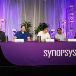
Four panelists from big-name semiconductor design companies spoke about their circuit simulation experiences at #53DAC in Austin this year, so I attended to learn more about SPICE and Fast SPICE circuit simulation. I heard from the following four companies:
Continue reading “Circuit Simulation Panel Discussion at #53DAC”
Xilinx is Killing Altera!
At a recent outing with FPGA friends from days gone by, the long running Xilinx vs Altera debate has come to an end. The bottom line is that Xilinx has used the FUD (fear, uncertainty, and doubt) of the Intel acquisition quite effectively against Altera and is racking up 20nm and 16nm design wins at an alarming rate. It will be a while before they all hit HVM (high volume manufacturing) but it is coming, absolutely.
The question I have now is: Will Xilinx be acquired next?
The Intel acquisition of Altera became official in December of 2015 at a cost of $16.7B which was more than a 50% premium based on the stock price when the deal was announced. Altera is the second largest maker of programmable chips (FPGAs), Xilinx (XLNX) being the first.
Altera and Xilinx are fierce competitors in a two horse race for a $5B+ market with an expected CAGR of 8.4% from 2016 to 2020. It is widely recognized in the FPGA world that the vendor who is first to a new process node wins the commanding market share. This was proven when Altera overwhelmingly beat Xilinx to the 40nm process node. Altera was partnered with TSMC (TSM) and Xilinx was partnered with UMC (UMC), UMC stumbled at 40nm and took Xilinx down with them. Prior to 40nm Xilinx was the node leader.
After the 40nm debacle at UMC, Xilinx moved to TSMC (joining Altera) making it a level process node playing field. Xilinx then beat Altera to the 28nm process node by a matter of months and again beat Altera to the 20nm node by more than a year. Xilinx of course was awarded majority market share as a result.
Altera then switched their manufacturing to the new Intel Custom Foundry division for 14nm to better compete with Xilinx. This was a huge PR event as Altera and TSMC were intimate partners since the beginning of the fabless semiconductor transformation in the 1980s. This also brought a direct competition spotlight on Intel versus TSMC for the first time.
Unfortunately Altera stumbled at 14nm and is hoping for high volume manufacturing (HVM) before the end of 2016 while Xilinx started 16nm HVM in 2015. Xilinx also has access to the low cost TSMC 16FFC process to which Intel has no answer so look for additional market share to be won by Xilinx moving forward.
The next process node is 10nm which Intel is currently delaying while TSMC will start 10nm HVM in the first half of 2017 with a quick step to 7nm HVM one year later. Given that quick step, Xilinx has chosen to skip 10nm and move directly to 7nm in 2018. As a result of the challenges Altera experienced with the Intel process bureaucracy at 14nm, I do not expect to see Altera in HVM at Intel 10nm until mid to late 2018, giving Xilinx another solid process advantage.
Will Xilinx be Acquired?
After Intel acquired Altera the rumors started about Xilinx being next. Really it was more about people, like myself, thinking out loud but I would not rule out due diligence and executive level discussions. My take is that Xilinx felt that the Intel/Altera acquisition would falter and favor Xilinx in the long run (which it already has). Xilinx is now in a much stronger position for acquisition discussions with companies that can leverage the dominant position they have in the high margin merchant FPGA market and the desire to compete with Intel in the data center business.
The first name that comes up in the media is Qualcomm but my bet is on Avago/Broadcom CEO Hock Tan. Hock has proven that he can make big deals happen (LSI Logic for $6.6B and Broadcom for a record $37B) and the data center business is in his sights, absolutely.
NVIDIA GeForce GTX 1080 Poised To Claim The Gaming And VR Performance Crown
NVIDIA has been teasing the promise of Pascal for years, but this year Pascal’s performance became much more real. With the announcement of the Tesla P100 based on Pascal, NVIDIA was able to show the neural-network world what Pascal was really capable of. However, that chip is very different from the gaming-focused Pascal chip that NVIDIA launched on May 6th in Austin at an event VR analyst Anshel Sag and I both attended. NVIDIA introduced a plethora of new features and improvements that enable their new Pascal-based GeForce GTX cards to really shine against the competition. NVIDIA’s own Founder and CEO, Jen-Hsun Huang, deemed the GTX “1080 is the new King.”
NVIDIA CEO Jen-Hsun Huang at the GeForce GTX 1080 launch event held in Austin, TX (Photo Credit: Patrick Moorhead)
GTX 1080 “firsts”
The Pascal GPU architecture is NVIDIA’s most ambitious ever. The biggest version of the Pascal family is the GP100 inside of the Tesla P100 high performance computing (HPC) GPU. That version of Pascal features 15.3 billion transistors, the most of any chip, ever created by anyone, ever. The newly announced GeForce GTX 1080 features the GP104 graphics chip with fewer transistors paired with 8GB of Micron GDDR5X, a brand new type of graphics memory. The improvements in memory bandwidth and latency mirror NVIDIA’s improvements in the Tesla P100 with the use of HBM2. However, while AMD didintroduce HBM in their Fiji family of GPUs, it was limited to 4GB of VRAM capacity and this new generation that NVIDIA is using does not have such a limitation. Additionally, AMD is not using GDDR5X anywhere in any of their cards, so NVIDIA is the first to introduce this technology to the market in a product.
16nm FinFET helping
The biggest reason why NVIDIA is able to cram so many transistors inside of a relatively small chip is thanks to the new 16nm FinFET process from TSMC. This process allows for NVIDIA to not only build a small chip but to pack it with plenty of performance and to do it at a very low wattage. In fact, NVIDIA claims to be cramming approximately 29% more performance out of the GeForce GTX 1080 than they do from their most powerful graphics card right now, the TITAN X. Not only is NVIDIA claiming to be about 29% faster than the previous generation, they are able to accomplish this with only 180 watts of power. This represents a power reduction of 28% while at the same time delivering a 29% boost in performance. Traditionally, GPU manufacturers have had to give up some power savings for additional performance or vice versa, but with the new Pascal architecture and 16nm FinFET from TSMC you get the best of both worlds.
VR-focused performance and features
The GeForce GTX 1080 delivers even more performance once you start looking at performance in Virtual Reality (VR). It appears the entire GTX 1080 and Pascal were specifically designed with VR in mind. This includes support for hardware asynchronous computing as well as some of their VR Works software features like simultaneous multi-projection (SMP). NVIDIA claims that with the added hardware and software features on the GeForce GTX 1080 actually bring its VR performance to approximately two times that of the TITAN X, NVIDIA’s next fastest graphics card.
However, in order to accomplish such performance, game developers have to implement NVIDIA’s Game Works proprietary SDK which includes their VR Works that enables the use of features like SMP. As many middleware programs go, the chance that it will be broadly adopted is to be determined, but there’s a good chance that there will be a handful of games that do and those that do could benefit from this performance boost. This is the promise of NVIDIA’s new technology inside of Pascal and the software that accompanies it. Plus, the VR industry is looking for anythingto boost the category, so I expect developers and game engines will support both SMP and Async. Already, VRWorks is integrated into game engines today with features like VR SLI supported.
Hardware Async compute
Prior to Pascal, NVIDIA’s Maxwell architecture supported asynchronous compute in hardware. Improvements to work scheduling in Pascal increases the overall performance in VR and improves the overall user experience allowing both compute and graphics functions to happen as they need to. This feature is extremely important in order to deliver a smooth VR experience and I suspect that NVIDIA knows this and has made sure their architecture supports it. NVIDIA prides themselves in the best possible gaming experience, so it only seems logical that they would want to deliver the best VR experience possible with the GTX 1080.
Exceptional pricing for high-end card
In addition to all of the features in the GeForce GTX 1080 that make it so VR friendly and power-friendly, NVIDIA’s new GPU is also extremely price friendly. The “Founder’s Edition” from NVIDIA comes in at a relatively low $699, which is a solid $400 less than their current top-end card the TITAN X, for more performance. NVIDIA also introduced the Founder’s Edition GTX 1070 that will be $379, which claims approximately TITAN X performance for about 1/3 the price. These new GPUs from NVIDIA deliver on performance, power and price, they are a complete win for virtually any gamer looking to spend more than $300 on a GPU. They will also deliver the best possible performance today, even if NVIDIA’s claims are overstated.
NVIDIA should continue to dominate over $300
NVIDIA is trying to capture the entire segment of the market above $300 that represents the “enthusiast segment”, which is about 20% of the overall GPU unit market volume and where the highest margins and revenue are. The biggest market segment is the “performance” segment which is below $300 and while it represents the most units sold this is where margins are thinner in this segment.
Unless something unforeseen happens, which I don’t think will happen, I believe NVIDIA should continue to dominate in this high ASP, lower units market above $300.
The real fight will be from $149- $299
GPU’s that are more than $150 and less than $300 are the sweet spot for unit volume and unit market share which is why NVIDIA will likely need to extend the GTX 1000 family down to something like a GTX “1060” soon. This will be especially important for NVIDIA because Advanced Micro Device’s upcoming Polaris GPU will likely be squarely aimed at this price segment in order to recapture unit market share and potentially profits. After all, this is Advanced Micro Device’s self-proclaimed “year of graphics”.
If NVIDIA can successfully launch and price a GTX “1060” within this price segment they can defend their market share from Advanced Micro Devices in this price point, even if they effectively own the high-end. NVIDIA’s market share position is strong right now, but they already have a pretty strong command of the high-end and that’s why it’s important that they can launch into the lower price segments as well.
While AMD hasn’t yet launched Polaris, I believe it’s going to be an absolute fight from $149 to $299, so get ready for it.
Wrapping up
The NVIDIA GeForce GTX 1080 and GTX 1070 are absolutely marvels of engineering from a company that knows what gamers want and who has been executing incredibly for the last few years. The company are delivering on the promise of Pascal and 16nm FinFET and they are even doing all of this while bringing down the price of their GPUs compared to the previous generation.
These new cards are important for the PC VR category as they radically improve the price-experience curve. While HTC is delivering and Oculus has been choking, at least we know that higher-end VR will look much better from a graphics perspective.
NVIDIA’s launch of the GTX 1080 has been extremely well received by gamers around the world and those who wish to see high performance and lower cost VR solutions. NVIDIA has without a doubt introduced what appears to be the fastest GPU for VR and it will be interesting to see how it actually stacks up in real world scenarios.
Thankfully, NVIDIA has provided us with a GTX 1080 in order for us to test their claims ourselves. NVIDIA has finally, fully committed themselves to VR and they don’t appear to be stopping any time soon, I expect to see more announcements in the VR space from NVIDIA as they continue to push Pascal through their different product lines.
TSMC Update at #53DAC!
TSMC is having an interesting year for sure. I was at the TSMC Symposium in Hsinchu last week and everyone was talking about the new 16FFC process. Silicon is out and it is exceeding expectations leading some people (me included) to believe that TSMC 16FFC will be the next TSMC 28nm in regards to popularity. To be clear, 16FFC is currently the “BEST” process node in regards to PPPA (price, performance, power, and area) available today, absolutely.
The proof is in the pudding of course and that pudding will arrive via the iPhone 7 this fall and yes, I am buying an iPhone 7 Pro to match my iPad Pro which I use every day. Netflixing on an iPad Pro at 30,000+ feet, priceless! It should have a “TSMC Inside” sticker on it for sure.
Speaking of FinFETs, we have published 64 FinFET related blogs thus far starting with Tom Dillinger’s three part Introduction to FinFET Technology series. The total views for the SemiWiki FinFET blogs exceeds 500k which is a lot of reading. FinFET blogs also have low bounce rates and high time-on-page numbers which means they are very engaging. Designing with FinFETs is still a hot topic so there are certainly more blogs to come.
At DAC, TSMC pioneered the partner theater allowing the fabless semiconductor ecosystem to shine, and this year it will be no different. You can see the latest TSMC Theater schedule HERE. If you are looking for me on the DAC exhibit floor that would be a good place to start. Or wherever there is free food.
Speaking of free food, TSMC is also very busy with other DAC activities that should be of interest. You can see the agenda HERE and please note that it includes breakfast, lunch, and dinner presentations so you can also find me there enjoying the free food.
As a pre #53DAC “Designing with FinFET” primer you should catch the TSMC and Solido Collaborate for Variation-Aware Design of Memory and Standard Cell at Advanced Process Nodes webinar on Wed, June 1st, 2016 10:00 AM – 11:00 AM PDT. If the time does not work for you, sign up anyway and they will send you a link to the replay:
“Variation effects have an increasing impact on advanced process nodes, and at each, new sources of variation must be considered. Furthermore, increased competition is forcing tighter design margins to make high-performance, low-power, low-cost products. Designers must now do more variation analysis than ever to achieve these tighter margins, using advanced variation-aware technology for speed, accuracy and coverage to deliver competitive chips on schedule.
This webinar will discuss how TSMC and Solido collaborate to offer variation-aware design techniques for memory and standard cell with TSMC advanced processes using Solido’s new Variation Designer 4.”
And don’t forget that SemiWiki will again be hosting a DAC Networking reception on Wednesday night from 6:00pm to 7:00pm in the Trinity Street Foyer. This year we will be giving away copies of our new book “Prototypical”. My beautiful wife and I hope to see you there!