You are currently viewing SemiWiki as a guest which gives you limited access to the site. To view blog comments and experience other SemiWiki features you must be a registered member. Registration is fast, simple, and absolutely free so please,
join our community today!
WP_Term Object
(
    [term_id] => 158
    [name] => Foundries
    [slug] => semiconductor-manufacturers
    [term_group] => 0
    [term_taxonomy_id] => 158
    [taxonomy] => category
    [description] =>
    [parent] => 0
    [count] => 1350
    [filter] => raw
    [cat_ID] => 158
    [category_count] => 1350
    [category_description] =>
    [cat_name] => Foundries
    [category_nicename] => semiconductor-manufacturers
    [category_parent] => 0
    [is_post] =>
)
– Intel announced 2 new fabs & New Foundry Services
– Not only do they want to catch TSMC they want to beat them
– It’s a very, very tall order for a company that hasn’t executed
– It will require more than a makeover to get to IDM 2.0
Intel not only wants to catch TSMC but beat them at their own … Read More
Intel made a big splash on March 23, 2021 by doubling down on manufacturing with the creation of Intel Foundry Services (IFS). The big announcement was supported by potential customers such as Qualcomm, Cisco, Ericsson, Google, Amazon, Microsoft, and IBM. With an accompanying $20B investment, the EDA and equipment industries,… Read More
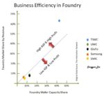
In January I presented at the ISS conference a comparison of Intel’s, Samsung’s and TSMC’s leading edge offerings. You can read a write-up of my presentation here.
With the problems going on at Intel, that article generated a lot of interest in the investment community, and I have been holding a lot of calls with analysts who are trying… Read More
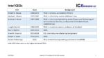
New Intel CEO Pat Gelsinger is not wasting any time in changing the course of the largest semiconductor company the world has ever seen. Today he announced the IDM 2.0 strategy which will better leverage Intel’s manufacturing abilities. There is a lot to talk about here but let’s focus on the new Intel Foundry Services because the… Read More
Dan takes an in-depth look at Intel with Stacy Rasgon, Managing Director and Senior Analyst, U.S. Semiconductors at Bernstein Research. Stacy is an unusual semiconductor analyst as he holds a Ph.D. in chemical engineering from MIT. His substantial technical knowledge allows for a deep dive on Intel that you will find refreshing… Read More
The term von Neumann bottleneck is used to denote the issue with the efficiency of the architecture that separates computational resources from data memory. The transfer of data from memory to the CPU contributes substantially to the latency, and dissipates a significant percentage of the overall energy associated with … Read More
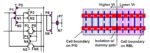
All-Digital In-Memory Computingby Tom Dillinger on 03-15-2021 at 6:00 amCategories: Events, Foundries, TSMC
Research pursuing in-memory computing architectures is extremely active. At the recent International Solid State Circuits conference (ISSCC 2021), multiple technical sessions were dedicated to novel memory array technologies to support the computational demand of machine learning algorithms.
The inefficiencies associated… Read More
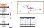
Register File Design at the 5nm Nodeby Tom Dillinger on 03-10-2021 at 2:00 pmCategories: Events, Foundries, TSMC
“What are the tradeoffs when designing a register file?” Engineering graduates pursuing a career in microelectronics might expect to be asked this question during a job interview. (I was.)
On the surface, one might reply, “Well, a register file is just like any other memory array – address inputs, data inputs and outputs, read/write… Read More
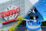
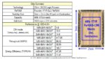
There are reports in the media that TSMC is now planning six Fabs in Arizona (the image above is Fab 18 in Taiwan). The original post I saw referred to a Megafab and claimed six fabs with 100,000 wafers per month of capacity (wpm) for $35 billion dollars. The report further claimed it would be larger than TSMC fabs in Taiwan.
This report… Read More
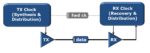
At the recent ISSCC conference, Mozhgan Mansuri from Intel gave an enlightening (extended) short course presentation on all thing related to clocking, for both wireline and wireless interface design. [1] The presentation was extremely thorough, ranging from a review of basic clocking principles to unique circuit design … Read More


Intel, Musk, and the Tweet That Launched a 1000 Ships on a Becalmed Sea