The next transition from current FinFET devices at advanced process nodes is the “nanosheet” device, as depicted in the figure below. [1]
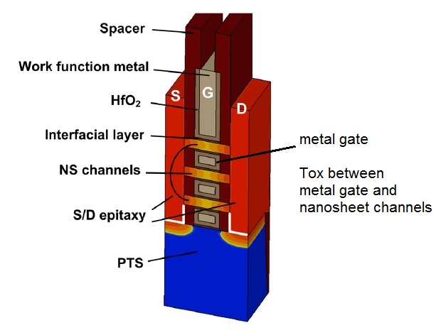
The FinFET provides improved gate-to-channel electrostatic control compared to a planar device, where the gate traverses three sides of the fin. The “gate-all-around” characteristics of the nanosheet device provide further improvements in electrostatic control, surrounding the device channel. This is typically reflected in a more optimal subthreshold slope, or SS. The SS relates to the change in device gate input voltage that results in a factor of 10X change in leakage current. A smaller SS implies both faster device switching and, significantly, a reduction in the static source/drain leakage current and leakage power dissipation. (More on SS shortly.)
Additionally, the nanosheet device offers more design flexibility. Whereas the topology of the FinFET device width is quantized (Weff ~ ((2*fin_height) + (fin_thickness))), the width of the nanosheet device is defined by EUV lithography (Weff ~ nanosheet_perimeter).
The effective nanosheet width can be further extended by stacking multiple channels vertically, with the gate material fully surrounding each of the individual nanosheets. The design flexibility and improved device characteristics make this technology option very attractive.
There are major challenges to the introduction of nanosheet processing to production, however. Here are but a few:
- isolation of individual “ribbons” of the nanosheet device channel
The nanosheet device is fabricated in an epitaxial layer. The horizontal device sheet is embedded within other epitaxial-grown layers – e.g., a silicon layer sandwiched by epitaxial layers of different composition, such as SiGe/Si/SiGe/Si/SiGe. (As will be described shortly, the close similarity in crystalline structure between Si and Ge is critically important.)
The formation of the nanosheet device “ribbon” requires a very selective etching process. The epitaxial layers above and below are to be removed, while not etching the remaining device channel. For multiple, stacked nanosheets, this etching process also needs to be anisotropic, so that all the sacrificial epitaxial layer material between nanosheets is fully removed.
- the high-K gate oxide dielectric surrounding the exposed nanosheet ribbons needs to be extremely uniform, with excellent adherence
The oxide defect density and interface trap density (for injected “hot” carriers) needs to be extremely low. (An annealing step in a hydrogen gas environment is commonly included as part of the device process flow.)
- similarly, the metal gate material stack needs to be deposited uniformly throughout the structure, fully enclosing the stacked sheets
The gate stack is typically comprised of an initial metal-to-oxide “workfunction” layer (e.g., TiN), followed by a metal to fill the gate volume, such as Tungsten. (Atomic layer deposition (ALD) is truly an amazing technology.)
- a low resistance source/drain device node needs to be fabricated adjacent to the channel, to reduce Rs and Rd
An epitaxial growth step (with a high dopant concentration) is used to increase the S/D volume next to the channel, suitably isolated from the gate by a sidewall separation oxide. (Other FET topologies also use a similar raised S/D epitaxial step.) Additionally, the S/D doping profile needs to ensure a low contact resistance to the first-level metal.
- “device engineering” needs to introduce significant strain into the channel material, to improve the free carrier mobility, and thus, the drive current
For several process generations, from planar to FinFET device topologies, various techniques have been employed to introduce strain into the channel material crystal – tensile strain for higher nMOS electron mobility, compressive strain for higher pMOS hole mobility. “Stressor” material dielectric layers were added on top of planar devices. The raised S/D epitaxial regions also transfer strain to the channel.
Of particular concern is the disparity between the electron and hole mobility in silicon. Process development engineers continually strive to improve the hole mobility, to bring it closer to the electron mobility. A key advance in this area has been the addition of Ge to the S/D epitaxial growth step, and ultimately, to the pFET channel – i.e., a Si(x)Ge(1-x) crystalline structure, providing a compressive strain and vastly improved hole mobility. (Seasoned circuit design veterans will remember the days when pFET device widths were 2.5X-3X the nFET device width, to compensate for the hole versus electron mobility disparity. With strain introduced during SiGe pFET fabrication, that difference is vastly reduced.)
The transition to a nanosheet channel of very small thickness exacerbates the difficulty in providing improved pFET device characteristics. At the recent IEDM conference, Intel presented a detailed paper on how their nanosheet engineering has addressed this challenge. [2] The rest of this article summarizes the highlights of their presentation.
pFET Nanosheet Fabrication
An overview of the nFET and pFET nanosheets are depicted in the figure below.
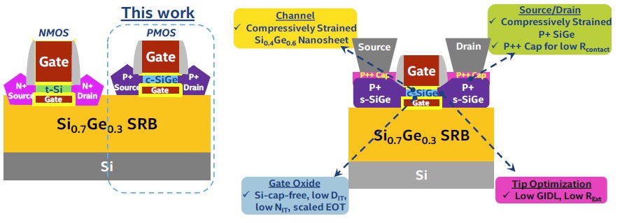
(The focus of the IEDM Intel presentation was on pFET engineering.)
As mentioned above, compressive strain in the channel is key to a high-performance device. This is achieved by the following:
- the epitaxial nanosheet for the pFET channel is Si(0.4)Ge(0.6)
- the raised S/D epitaxial growth volume is also SiGe
- the substrate directly below the nanosheet consists of Si and a “strain relief buffer” (SRB) layer of Si(0.7)Ge(0.3)
This buffer layer offers an intermediate crystalline transition from the bulk silicon substrate, and provides some degree of additional channel strain.
Parenthetically, the crystal lattice constants of Si and Ge differ by only 4.2% — Si = 0.543nm, Ge = 0.566nm. As a result, the Ge/Si ratios are fully miscible.
The figure above also illustrates other process engineering constraints:
- a highly doped top layer on the S/D regions is required for low contact resistance
- the gate oxide needs a low defect and trap density (with a very aggressive high-K material thickness – e.g., an interface dielectric to the channel and a subsequent HfO2 layer)
The transition from the nanosheet thickness (~5nm) to large p+ S/D nodes requires detailed process engineering, to electrically isolate the gate from the S/D, and introduce compressive strain into the pMOS channel from the doped SiGe epitaxy. (More on this step shortly.)
The figure below summarizes the overall Intel pMOS nanosheet fabrication steps, and provides a TEM cross-section of a single nanosheet device – NS thickness = 5nm, Lgate = 25nm, width = 100nm, EOT oxide = 9.1Angstroms.
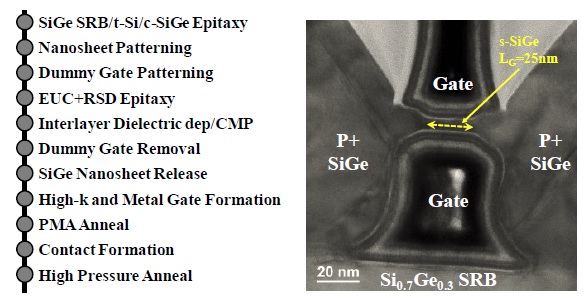
Nanosheet fabrication requires several unique steps, combining conformal materials deposition with both isotropic and anisotropic (directional) etch technology. Additionally, the isotropic etch technology needs to be very selective to different materials composition.
The figures below from Reference [3] illustrate an overall flow for the general case of multiple stacked nanosheets. (The Intel IEDM discussion focused on materials and compressive channel strain for a single pMOS nanosheet device.)
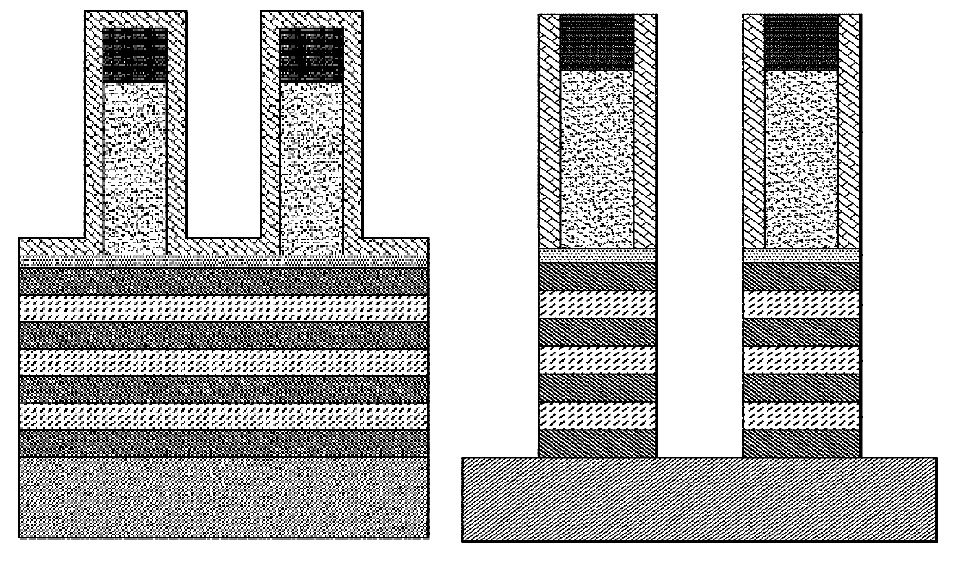
The starting material is alternating layers of undoped Si/SiGe epitaxy. A “dummy” top-level gate is patterned, followed by conformal deposition of an oxide and (highly) anisotropic etching of the oxide and Si/SiGe layers to form the starting nanosheet stack. The next steps are critical, as depicted below.
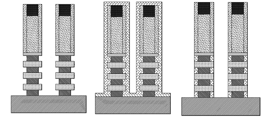
The sidewalls of the exposed gate areas are selectively etched, to provide a recessed volume for conformal oxide deposition. Anisotropic etching of this oxide results in a stack where the gate areas have lateral spacer oxide, while the sidewalls of the channels remain exposed, and serve as the seed for source/drain epitaxial growth.
Nanosheet nMOS devices in Si require processing with highly selective etching of the adjacent SiGe layer, exposing the Si sidewall for S/D epi growth. Nanosheet pMOS devices require high etch rates of Si, exposing the SiGe sidewall for S/D epi growth. Extensive process R&D (and materials chemistry) has been applied to optimize the Si/SiGe “etch rate ratios”.
After S/D epi growth, the dummy gate and epitaxial gate layer are etched away (again, very selectively to the now released nanosheet channel “ribbons”). After a pre-clean, the high-K gate oxide materials are deposited on the ribbons, followed by the (workfunction and low-resistance) metal gate stack, both steps using atomic-layer deposition (ALD). Contact “trenches” down to the bottom nanosheets are opened and filled with metal, completing the nanosheet fabrication. (There are chemical-mechanical polishing (CMP) steps in this flow, as well, for surface planarity prior to etching.)
Parenthetically, it should also be mentioned that extensive process R&D has been invested to select the specific crystalline orientation that optimizes the strain-enhanced carrier mobility, etch rate selectivity, and S/D epitaxial growth.
Nanosheets and the parasitic transistors
Returning to the Intel presentation for their optimized compressive strain pMOS nanosheet, IDS-VGS curves for different devices are shown below (Lgate = 55nm and 25nm).
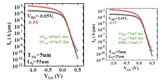
As might be expected from the superior electrostatics of the gate-all-around configuration, the subthreshold slope measured for these devices is exceptional. (Intel did not describe their engineering approach toward establishing the threshold voltage of the pFET device.)
Of particular interest is the behavior at the S/D-to-substrate interface. The nanosheet structure results in a parasitic transistor between the metal gate surrounding the bottom nanosheet and the substrate. The S/D contact to the nanosheet also serves as the S/D connection for the bottom parasitic transistor. To evaluate the magnitude of this parasitic device current, Intel fabricated and measured a test vehicle consisting of only this parasitic transistor – the experimental results are shown below.
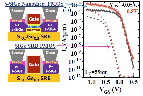
The leakage currents from this device are much less than for the nanosheet, indicating suitable suppression of this “sneak” current. (To further reduce this parasitic current, a punchthrough stop dopant region could be introduced below the S/D contact.)
VDD Optimization
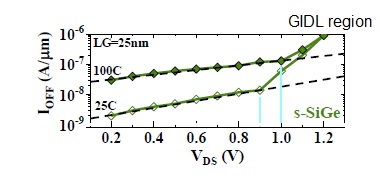
For high-performance applications, designers are seeking to boost the supply voltage toward the technology maximum. The limitations are due to the increased Ioff leakage at higher voltages. A higher drain-to-source electric field in the channel result in drain-induced barrier lowering (DIBL) current, and very high drain-to-gate fields result in gate-induced-drain-leakage tunnel current (GIDL). The figure below indicates that VDD = 0.9V is feasible for this technology, before the GIDL current increases exponentially (strained-SiGe, Lgate = 25nm, t_NS = 5nm).
Summary
Nanosheet devices are the next evolution in advanced process nodes after FinFETs. Yet, nanosheet fabrication requires several unique process steps – e.g., ALD, epitaxial growth, and highly selective etch rate ratios. Of specific concern is the requirement to introduce compressive strain in the pMOS nanosheet channel, to improve the hole mobility. A unique combination of Si and Si(x)SiGe(1-x) material layers and epitaxy are required. Intel recently discussed their results on optimizing pMOS nanosheet engineering. I would encourage you to review their presentation.
-chipguy
References
[1] Jeong, J., et al, “Comprehensive Analysis of Source and Drain Recess Depth Variations on Silicon Nanosheet FETs for Sub-5nm Node SoC Application”, IEEE Access, Volume 8, 2020.
[2] Agrawal, A., et al, “Gate-All-Around Strained Si0.4Ge0.6 Nanosheet PMOS on Strain Relaxed Buffer for High Performance Low Power Logic Application”, IEDM 2020, paper 2.2.
[3] Cheng, K., et al., “Nanosheet with Changing SiGe Percentage for SiGe Lateral Recess”, US Patent No. 10,312,350B1, June 4, 2019.
Share this post via:


Comments
3 Replies to “Optimization for pFET Nanosheet Devices”
You must register or log in to view/post comments.