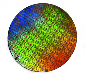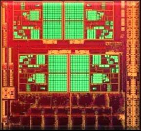
The GlobalFoundries Technical Conference last week was one of the best I’ve seen. The theme of the conference was “GlobalFoundries is bringing the collaborative IDM semiconductor design and manufacturing culture to the merchant foundry business!”
“We ramped volume production at the 45/40nm node well ahead of all foundries and we are poised to maintain this leadership at 32/28nm, with plans to extend this to the 22/20nm node.”
Gregg Bartlett, Senior VP of technology and R&D, did one of the most complete technology reviews I have seen, in 28 minutes! I was even afforded time with Gregg for follow-up questions after his presentation (the benefits of being a world famous blogger!).

Thus far, GFI has executed an incredible marketing and PR campaign, taking full advantage of TSMC, UMC, and SMIC’s conservative culture. My first concern is can GFI implement technically, especially in regards to yield? My second concern is can GFI offer competitive pricing and capacity? As we all know in the wafer business, pricing and delivery trumps all.
The most significant announcement at the conference was a very aggressive 32nm/28nm and 22nm/20nm roadmap. So in addition to supporting multiple versions of 45nm SOI, 40nm CMOS, and 32nm SOI, GFI will beat TSMC to multiple versions of 28nm and 20nm?

The gate-first versus gate-last issue also came up. GFI claims that gate-first will offer a 15-20% die area advantage over gate-last. Gate-first will also allow existing design practices. During a discussion with Dr. S.Y. Chiang, the senior vice president at TSMC in charge of R&D, I was told that a gate-last approach with restricted design rules would yield much better. Dr. Chiang also predicted that 20nm will require the gate-last approach due to added complexities. I asked Gregg Bartlett twice what gate strategy GFI would use at 20nm and was unable to get a clear answer.
he other interesting announcement was the GFI 28nm AMS reference flow:
“GLOBALFOUNDRIES has joined with Cadence to deliver the major elements of the AMS production design flow in Q3, 2010, with all of the flow steps supported by the GLOBALFOUNDRIES PDK. The reference flow contains PCells that enable critical advanced features within Cadence Virtuoso custom design tools. The complete production-level AMS flow is expected to be released to customers in Q4 2010, with silicon validation scheduled for early 2011.”
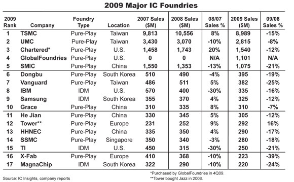
Another interesting thing I learned at the conference was revenue. Being a private company has distinct advantages, such as no required financial disclosures, but the GFI CEO did mention revenue. The combined AMD and Chartered manufacturing operations did $2.5B in revenue last year. In 2010, Doug Grose estimated $4B, which would put GFI in contention for the #2 slot with UMC. Given the technology road map, IDM like collaboration, deep pockets, and aggressive marketing and PR, I would put GFI in contention for #1 with TSMC.


Musk’s Orbital Compute Vision: TERAFAB and the End of the Terrestrial Data Center