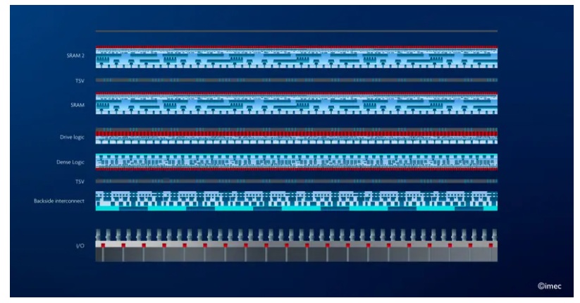
In the rapidly evolving semiconductor landscape, imec’s recent breakthroughs in wafer-to-wafer hybrid bonding and backside technologies are reshaping the future of compute systems. As detailed in their article, these innovations transition CMOS 2.0 from a conceptual framework to practical reality, enabling denser, more efficient chip architectures. Presented at the 2025 VLSI Symposium, imec demonstrated hybrid bonding at a 250nm interconnect pitch and backside through-dielectric vias (TDVs) at 120nm pitch, marking significant milestones for stacking functional tiers in system-on-chips (SoCs).

CMOS 2.0 represents a paradigm shift in CMOS scaling, addressing the diversification of computational demands from AI to mobile applications. Traditional general-purpose CMOS struggles with these varied needs, prompting imec to propose partitioning SoCs into heterogeneous functional layers via system-technology co-optimization (STCO). Each layer is tailored to its role—high-drive logic for performance, high-density logic for efficiency, or memory integration. These tiers are interconnected using advanced 3D technologies, with backside power delivery networks (BSPDNs) decoupling power from signal routing to minimize voltage drops and congestion.
A cornerstone of this approach is wafer-to-wafer hybrid bonding, which provides sub-micron pitches for logic-on-logic or memory-on-logic stacking. Imec’s roadmap spans from ball grid arrays to ultra-fine BEOL-like densities. The process involves etching cavities in dielectric layers (typically SiO2 or SiCN), filling with copper, and polishing for flatness. Wafers are aligned and bonded at room temperature, followed by annealing for permanent Cu-to-Cu bonds. At IEDM 2023, imec achieved reliable 400nm pitch connections with high yield, using SiCN for better strength. Pushing further, they now target 200nm pitches, tackling overlay challenges through simulations of bonding wave distortions and pre-bond litho corrections. The 250nm pitch demo at VLSI 2025, with TEM images of daisy chains, highlights feasibility, though next-gen equipment is needed for full-wafer yields.
Complementing frontside bonding, backside connectivity enables dual-sided access, crucial for multi-tier stacks. Imec’s nano-through-silicon vias (nTSVs) connect front and back metals seamlessly. Their VLSI 2025 work featured barrier-less molybdenum-filled TDVs with 20nm bottom diameters at 120nm pitch, fabricated via a via-first approach in shallow-trench isolation. Extreme wafer thinning ensures low aspect ratios, while higher-order lithography corrections achieve 15nm overlay margins. These vias minimize standard cell area usage, supporting direct transistor access for power or signals.
BSPDNs further amplify benefits, routing power from the backside to reduce IR drops and free frontside BEOL for signals. Imec’s DTCO studies show PPAC gains in always-on designs, but the 2025 VLSI paper extends this to switched-domain architectures for power-managed mobile use. Comparing 2nm mobile processors, BSPDNs cut IR drops by 122mV, allowing fewer power switches and 22% area reduction versus frontside PDNs. Power switches in checkerboard patterns distribute switched VDD efficiently, enhancing performance in constrained environments.
These technologies converge in CMOS 2.0, fostering heterogeneity within SoCs akin to chiplets but at finer granularity. By enabling tier stacking with cell-level connectivity, they overcome scaling bottlenecks, benefiting fabless firms and system designers. Imec’s ecosystem collaborations, including the NanoIC pilot line funded by EU programs, underscore collaborative progress.
In conclusion, imec’s path to high-density connectivity heralds a new era of compute scaling. Hybrid bonding and backside vias not only realize CMOS 2.0 but promise energy-efficient, high-performance systems. As published in Chip Scale Review (July/August 2025), these advancements invite broader adoption, driving innovation across the semiconductor value chain.
Share this post via:


Musk’s Orbital Compute Vision: TERAFAB and the End of the Terrestrial Data Center