


The 2026 Ceva Edge Symposium will bring together engineers, technology leaders, ecosystem partners, and innovators to explore a major shift in computing: moving artificial intelligence from distant cloud infrastructure into the devices that interact directly with the physical world. Scheduled for November 2 in Hsinchu,… Read More
Jensen Huang and the Cost of Unchecked InfluenceAs a semiconductor professional with 45 years in…Read More
CTO Interview with Juan Rey, senior VP and general manager of Calibre and CTO of Siemens EDAJuan Rey is Head of Technology and Innovation…Read More
CTO Interview Kevin Robinson, VP of Operations, yieldHUBKevin Robinson is VP of Operations at yieldHUB,…Read More
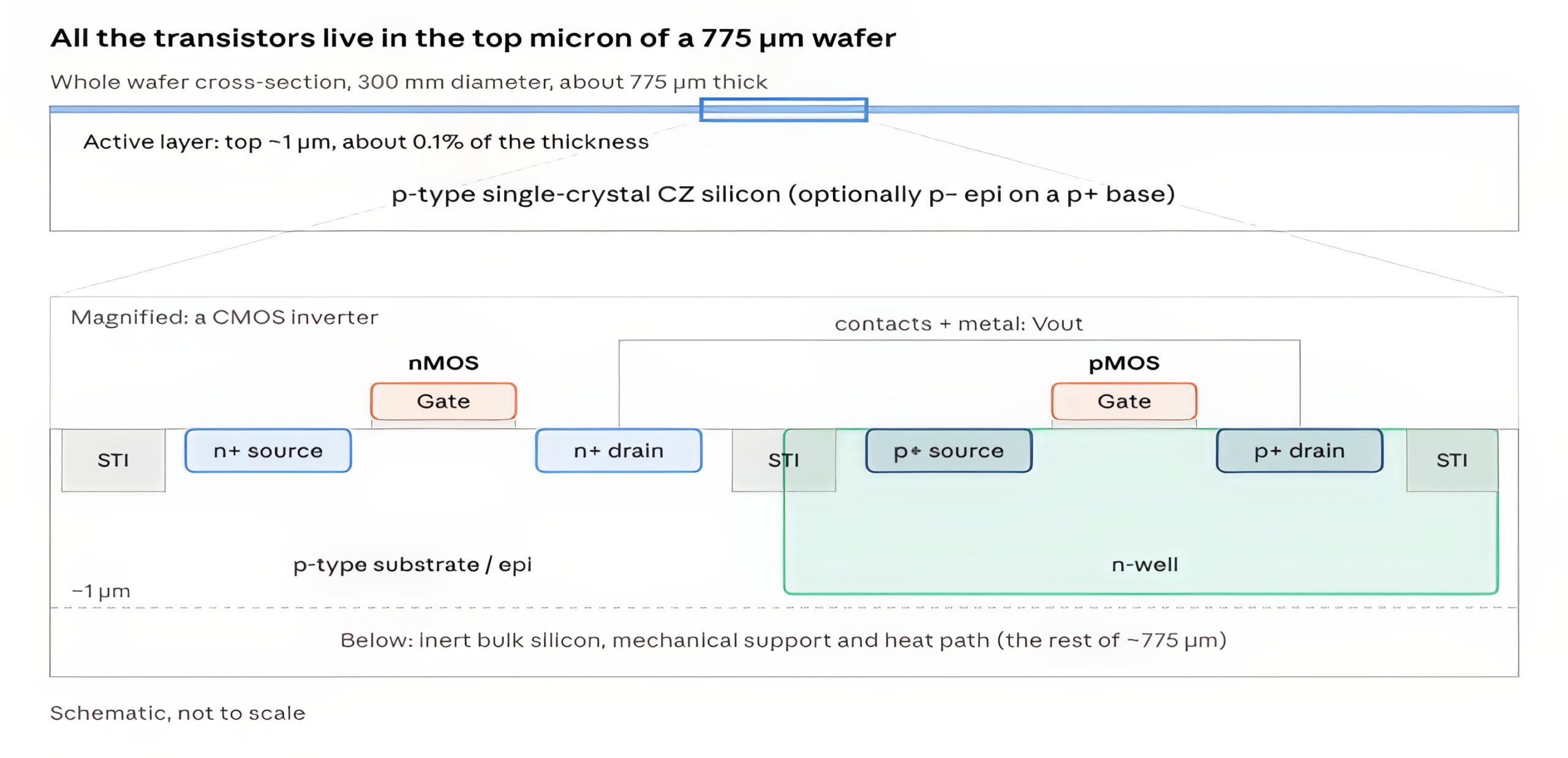
Semiconductors and SOI: From Bulk Wafers to Engineered Substrates1. Why the substrate matters Every transistor sits…Read MoreHBM’s Second Act: When Memory Starts Thinking
Samsung’s Hot Chips 2026 presentation, “HBM Base Die: How HBM Will Evolve Using Advanced Logic Processes,” argues that the base die beneath a High Bandwidth Memory stack is about to become far more than a communications layer. Traditionally, an HBM base die mainly connects stacked DRAM dies to a GPU, TPU, or other processor and … Read More
NVIDIA Vera: Rebuilding the CPU for Agentic AI
Source: Jonathon Evans and Polychronis Xekalakis, “NVIDIA Vera CPU,” Hot Chips 2026. Performance figures are NVIDIA claims, and several results were based on preproduction or unofficial testing.
NVIDIA’s Vera CPU is a server processor designed specifically for agentic AI, where language models repeatedly observe, reason,… Read More
Fail-Safe Frames: Why Chips&Media’s ASIL-B Video IP Matters
As vehicles evolve into software-defined, increasingly autonomous platforms, video processing is becoming part of the safety-critical computing chain. Camera feeds support functions ranging from surround-view monitoring and driver assistance to object detection and automated driving. If the hardware processing those… Read More
High-NA EUV Moves From Experiment to Manufacturing
Intel Foundry and ASML say high-numerical-aperture extreme-ultraviolet lithography has crossed an important boundary: it is no longer only a development tool, but a production technology. At the SPIE Photomask Technology and Extreme Ultraviolet Lithography conference, the companies reported that Intel has processed … Read More
ASML and TSMC’s 12-Inch Photomask Initiative: Technical Significance
ASML and TSMC’s proposed shift from 6-inch to 12-inch photomasks is an attempt to redesign a critical but often overlooked part of advanced semiconductor manufacturing. Photomasks are precision plates carrying the circuit patterns projected by a lithography scanner onto a silicon wafer. In extreme-ultraviolet lithography,… Read More
When Design Gets Faster, the Bottleneck Moves Through the Physical Stack
AI can compress the path to tape-out. The next challenge is compressing physical realization.
Something important is beginning to happen in semiconductor development: the design cycle itself is becoming compressible.
AI-assisted engineering can accelerate architecture exploration, RTL development, verification, physical… Read More
Comparing Advanced Packaging from TSMC, Intel Foundry, and Samsung Foundry
Advanced semiconductor packaging has become essential to improving computing performance as conventional transistor scaling grows more difficult and expensive. Instead of manufacturing an entire processor as one large monolithic die, chipmakers can divide it into smaller chiplets and combine logic, memory, input/output… Read More
CEO Interview with Sander den Hoedt of Delmic
Sander is an Applied-physics graduate from TU Delft. Worked at a semiconductor start-up during his studies, decided building a company would be the most interesting way to shape his career. In 2010, a TU Delft professor suggested combining light and electron microscopy. Sander and co-founder Andries Effting took the patent … Read More
Semicon West: Transforming Tomorrow One Chip at a Time
SEMICON West 2026 arrives at a pivotal moment for the global chip industry. Scheduled for October 13–15 at San Francisco’s Moscone Center, the event returns to the Bay Area after its 2025 edition in Phoenix. Organized by SEMI under the theme “Transform Tomorrow,” it will bring together semiconductor manufacturers, equipment… Read More


Jensen Huang and the Cost of Unchecked Influence