Machine Learning (ML) has become extremely important for many computing applications, especially ones that involve interacting with the physical world. Along with this trend has come the development of many specialized ML processors for cloud and mobile applications. These chips work fine in the cloud or even in cars or phones, but they are nowhere miserly enough when it comes to power consumption for use in IoT applications. For instance, many automotive ML processors use between 100W and 500W. Edge devices such as phones can get by with one tenth of a watt, but to go into what Eta Compute calls the extreme edge, power consumption has to be in the realm of 1 to 10mW.
Let’s look at some extreme edge applications and why it is useful to have ML processing performed locally. IoT devices at the extreme edge will perform many sensor related tasks. Examples are thermostats, occupancy sensors, smoke detectors, etc. Included in this group are medical and fitness devices such as fitness bands, health monitors and hearing aids. For commercial applications we see things like asset tracking, retail beacons and remote monitoring. Many of these use small batteries and require long battery life. Some even rely on energy harvesting for power.
Looking at the list above it becomes clear how ML could be useful. Yet these devices cannot afford the energy budget to transfer raw data to the cloud for processing. There is also a cost saving to not relying on cloud processing for every IoT device that needs ML capabilities. Another benefit is the low latency achieved by saving a trip to the cloud for recognition tasks or even training. The solution is to build highly optimized ML processors for IoT and extreme edge usage.
This is exactly what Eta Compute has done with its announcement of their ECM3532 Neural Sensor Processor at the second TinyML Summit held in San Jose on February 12th. The ECM3532 is an SoC for ML and can be trained with the popular.

TensorFlow software. Their chip is especially interesting because it gains a huge efficiency advantage through their self-timed continuous voltage and frequency scaling (CVFS) technology. Because the control CPU and the DSP, which includes optimized MAC units, both use CVFS they are seeing a 10x reduction in power compared to traditional clocking and voltage supply approaches.
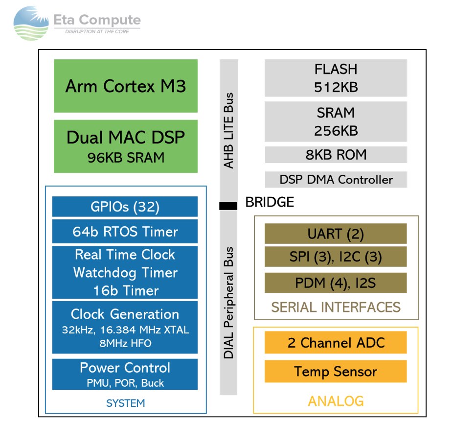
The ECM3532 contains an ARM Cortex-M CPU and a dual MAC 16-bit DSP. It also has onboard memory (Flash, SRAM, ROM), an ADC, serial interfaces, GPIOs, RTC, clock generation and power control. Running a variety of different benchmarks and applications, the ECM3532 is able to perform inference with less than 1mA of power consumption. Even when running COREMARK at up to 100 MHz its power consumption stays in the single digit mW range. The chip is capable enough, with 512KB of Flash and 256KB SRAM, for Eta Compute to provide demos in speech, image and video recognition, and industrial sensors. To provide flexibility in communication choices, the ECM3532 itself does not have onboard RF support, but it is expected to be designed into packages or boards with any desired wireless protocol chip or chiplet for cloud connectivity.
Because of their architecture choices on CPU, DSP and MAC, they are seeing excellent results in performance. On the CIFAR-10 CNN dataset they were able to reduce the number of operations required by a factor of 10 and reduce the weight size by 2 and achieve similar accuracy compared to published academic results.
Eta Compute is opening the doors to making IoT devices smarter and more responsive without drawbacks of shorter battery life or infeasible unit costs. Smarter IoT devices will offer more functionality and play a larger role in industry, medicine, appliances and elsewhere. It will be interesting to see the applications that are developed using this breakthrough technology. More information on their announcement can be found on the Eta Compute website.
Share this post via:


Silicon Insurance: Why eFPGA is Cheaper Than a Respin — and Why It Matters in the Intel 18A Era