I have a transistor-level IC design background so was intrigued to learn more from the CEO of an IP and services company that started out in India 12 years ago. Last week I spoke with Samir Patel, CEO of Sankalp Semiconductorabout the newest $5 million financial investment in his company from Stakeboat Capital Fund. The Stakeboat Capital Fund has some 28 years of investing experience and a current market capitalization above $8B.

I knew that the general trend was for IP companies to provide more specialized content along with design services to help speed new electronic products to market, but I didn’t realize that there are some 200 IC design services companies around the world competing for this growing market segment. What makes outsourced IC design services attractive to OEMs are:
- Lower cost of development than hiring and training new engineers
- Lower risk with a supplier that has a good track record
- Access to analog and mixed-signal IP blocks
Related blog – ARM’s back in FD-SOI. NXP’s showing real chips
Sure, there are giants in outsourcing like Wipro and Infosys, so what makes Sankalp interesting to me is their focus on analog and mixed-signal IP, something that is in strong demand these days as every IoT device with a sensor will require an AMS chip to get data into a digital format. The engineers at Sankalp have quite a broad range of experience to help speed the AMS parts or all of your next chip projects:
- Specification definition
- RTL design and verification
- SoC Implementation
- IP blocks
- AMS design
- Custom layout and P&R
- Technology Foundry Interface
- Validation and Characterization
Related blog – Can FD-SOI Change the Rules of the Game?
The success at Sankalp can be measured by the staff size with some 600 employees worldwide, serving tier one semiconductor companies. They can work with any foundry partner that you choose.
I learned that their logo shows two hands above a fire, and that Sankalp is a Sanskrit word meaning an oath or resolve. Instead of starting up the company in Bangalore, they located outside of Bangalore closer to engineering colleges and where they could train new hires at a lower cost and have lower attrition. TI was an early anchor client for them. Global locations include:
- India
- Noida
- Kolkata
- Bhubaneswar
- Hubli
- Bangalore
- Franfurt, Germany
- Ottawa, Canada
- Sunnyvale, CA
- Dallas, TX
Related blog – IP/SoC Rebound in 2015!
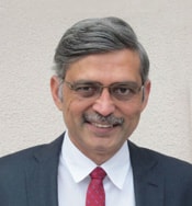
I did ask about exit plans or getting acquired by a larger firm, and was refreshed to hear that they will continue to grow and invest in their own success instead of cashing out. Past acquisitions include Interra SSG and KPIT SSG. Mr. Patel previously started up the RAMBUS design center in India, so really knows the semiconductor design industry. One new acronym that I heard for the first time was Application Specific System on a Chip (ASOC). I found Samir’s photo online and felt connected to him because we both have some grey hair and have followed the semiconductor industry for decades.

Share this post via:


Chemical Origins of Environmental Modifications to MOR Lithographic Chemistry