When I was not messing around with FPGA Research and Development, or Algorithms, I was often called into the lab or field and presented this type of scenario… Most of the time, the fix was the same…
At least a few times a year, I’d get the call. Sometimes a panic in the voice, or sometimes defeat. And who wouldn’t be defeated? After all, the FPGA design worked in PowerPoint :p and in ModelSim. The designers scrubbed and polished all the timing warnings and it was go time, excitement was in the air. The bosses were happy as earned value was thru the roof and believed that this FPGA was only going to be routed once! Then the worst case scenario was happening. “A Non Deterministic Timing Problem”… The panic would get so bad that the engineers would start using the ‘R’ word ‘RANDOM’, I wanted to patent their RANDOM design and just retire, but then I recalled the company was paying me to solve this problem.
So standing usually in front of some VME chassis, I would start asking a series of questions, like who did your hair? No, seriously I use humor to diffuse the much stressed, tired, cranky managers and engineers. Sometimes it even worked. I would ask:
- After a power cycle or cold start what happens?
- Has this problem always presented this way, i.e. , software change (hey, got to blame the software guys…)
- How long into the ‘run’ before the problem occurs?
- Is it repeatable? What has changed?
- Was the top level simulated?
- How many clock domains does the FPGA have?
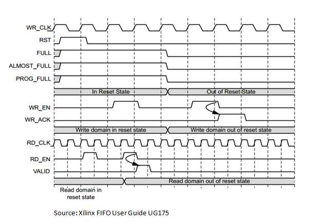
- Did you use Asynchronous FIFOs to cross those domains and use either an EMPTY FLAG or the like to push/pull data?
Believe it or not, those two last questions have solved most of the hard FPGA system integration type questions over my career. It was sometimes due to a fancy or green FPGA designer thinking he could design around the clock boundaries and not use asynchronous FIFOs. Other times it was the assumption on data rates. The designer thought that the FIFO would never go empty so why look. A great FPGA designer will always look at the data valid and empty flags. If the interface rates change, your design is robust enough to handle them without an FPGA re-spin.
With FPGA designs having easily 10 plus clock domains, it is ever important to pay attention and design ahead the FPGA clocking architecture. Use VISIO or a notebook, the point is put the keyboard down and prove to yourselves how you are going to synchronize all the data within that FPGA. This work lends to the old adage, ‘Ounce of prevention is worth a pound of cure’.
Share this post via:


Musk’s Orbital Compute Vision: TERAFAB and the End of the Terrestrial Data Center