Array
(
    [content] => 
    [params] => Array
        (
            [0] => /forum/threads/intel-foundry-gathers-customers-and-partners-outlines-priorities-intel-connect-live.22714/page-5
        )

    [addOns] => Array
        (
            [DL6/MLTP] => 13
            [Hampel/TimeZoneDebug] => 1000070
            [SV/ChangePostDate] => 2010200
            [SemiWiki/Newsletter] => 1000010
            [SemiWiki/WPMenu] => 1000010
            [SemiWiki/XPressExtend] => 1000010
            [ThemeHouse/XLink] => 1000970
            [ThemeHouse/XPress] => 1010570
            [XF] => 2021770
            [XFI] => 1050270
        )

    [wordpress] => /var/www/html
)

Intel Foundry Gathers Customers and Partners, Outlines Priorities (Intel Connect Live)

Btw I didn't hear a word about turbo cell is it similar to Nanoflex?

View attachment 3125
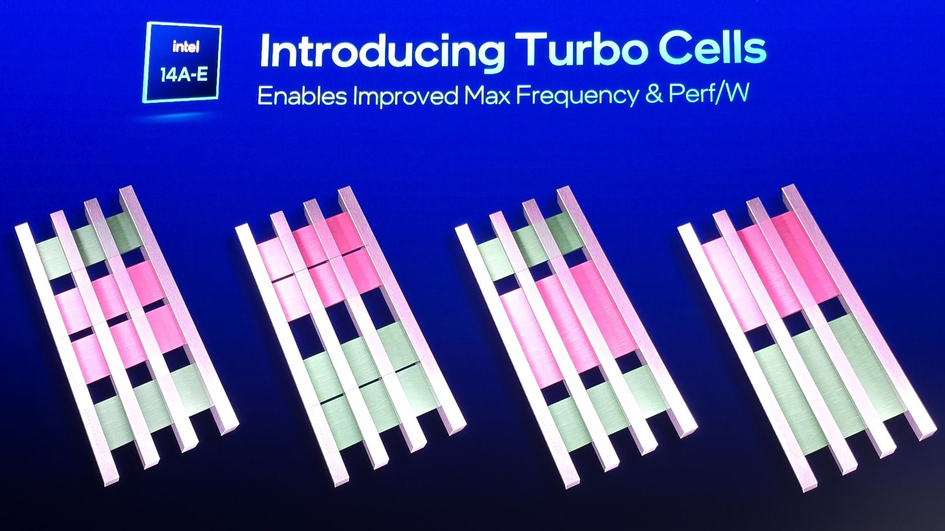

Short answer is yes, Intel's response to Nanoflex. You can mix high performance standard cells in with your standard or low power library. I do not remember cell height being mentioned but generally they are a few tracks taller (bigger transistors). Maybe 9 track versus 6 or 5 track? We used to have to choose between a high performance library versus a low power library or something in the middle. Now you can have a mix, tall cells for critical paths and smaller cells for better density/power.

TSMC has been showing N3 FinFlex benchmarks with Arm cores and they really are impressive. Nanoflex is for N2 but same principle. NanoFlex Pro is A14. Everything is on Youtube ;)

 
My experience is obviously colored by my experience with leading edge process R&D but I feel that verbage is far too dramatic and sensational for something so routine in manufacturing and in R&D.

My apologies, I thought you worked in marketing. I will let foundry customers know that their designs will be the same whether they use 14A with or without HNA-EUV. That will be such a relief. :ROFLMAO:
 
My apologies, I thought you worked in marketing.
I'm shocked you thought I was in marketing for these nearly 3 years. Not a dig at marketing people, but I figured the content of my posts and prior comments about my experiences in dry etch, process integration, and in semiconductor manufacturing kind of precluded me from being anything other than a process engineer of some kind.
I will let foundry customers know that their designs will be the same whether they use 14A with or without HNA-EUV. That will be such a relief. :ROFLMAO:
Maybe I am being as dense as a brick and I just don't get the joke, but Intel literally said that at the conference. And I doubt anyone who is working with Intel on 14A would already know that information. Considering TSMC said their plan was for A14P to use high-NA, I have to assume that TSMC's insertion will also be transparent to designers. I doubt they want another N7P vs N7+ situation where you are stuck designing to a non design rule compliant A14 or A14P.
 
I'm shocked you thought I was in marketing for these nearly 3 years. Not a dig at marketing people, but I figured the content of my posts and prior comments about my experiences in dry etch, process integration, and in semiconductor manufacturing kind of precluded me from being anything other than a process engineer of some kind.

I was joking. I'm an admin remember? I see all and know all, kind of like the Wizard of Oz. When did TSMC say their plan was to use HNA-EUV at 14P?
 
I attended the previous Intel Foundry event and spoke with Ann K and I remember her saying Intel could do 14A with or without HNA-EUV but the plan was 14A with HNA-EUV. Pat Gelsinger of course was full charge on 14A with HNA and Intel being first.

I did not see Ann at the event this week but this is the first time I have heard Intel say or show on a slide that they would release an EUV version of 14A. To me this is a bad sign for HNA-EUV.

Either way I am with TSMC on this one. HNA-EUV will not be ready for HVM anytime soon. TSMC has the benefit of building a consensus with the top foundry customers around the world and delivering what they decide on. If customers want BSPD TSMC will deliver. The same goes with HNA-EUV but it must pass the cost/risk test set by TSMC's customers.

Just my opinion of course.
I really believe the only reason that HNA-EUV is being discussed is because Gelsinger made a big deal out of it. If he hadn't tried to use it for bragging rights, it would be a non-issue.
 
So the oft-mentioned 40 steps is for the no High-NA contingency at 14A, then?
For the previously mentioned reasons from my earlier reply about it, that would be my assumption. Could be wrong, though.
I was joking. I'm an admin remember? I see all and know all, kind of like the Wizard of Oz.
Fair enough. Humor in text form is certainly harder to understand.
When did TSMC say their plan was to use HNA-EUV at 14P?
Apparently Kevin Zhang said it inside this interview linked in this post. This awful internet journalist don't make it clear when they are editorializing, speculating, and saying the words out of people's mouth. So maybe it is a load of BS. Can't read the thing for myself due to the paywall, so I have to rely on the summary that Fansink posted. FWIW an A14P insertion does sound plausible for any layers where there may be benefit. A14 HVM start is about two years after 14A HVM start (assuming Intel starts HVM in early 2027/late 2026 so they can launch 14A products at EOY 2027). By the time we are talking A14P and non Apple customers, we are talking about 3 years after 14A HVM start and 2 years after 14A/14A-E foundry start (assuming Intel sticks to their foundry roadmap) and we'd even be talking about Intel 10A HVM. By then, Intel should have broken high-NA in. If TSMC was to wait for A10 for high-NA, we would be talking about 2031 for first insertion, 5 years after Intel! At that point we might even see something comical like Micron using high-NA for DRAM before TSMC. Waiting that long would be like if Intel first adopted EUV on 18A. I just can't imagine TSMC waiting so long, even if high-NA is nowhere near as ready as Intel makes it out to be.

On a somewhat related note, TSMC extending the time between major processes to 3 years really does make things difficult. You go at the same pace or slower than someone doing 2-year gaps, and you fall behind. You accept the 3-year gaps and try for bigger bangs with each node, and you run the risk of delays. I really think TSMC just needs to have more than 2 leapfrogging process development teams so they can go back to 2-year gaps with the same amount of time as they do now (5 years) for a full process development cycle.
 
For the previously mentioned reasons from my earlier reply about it, that would be my assumption. Could be wrong, though.

Fair enough. Humor in text form is certainly harder to understand.

Apparently Kevin Zhang said it inside this interview linked in this post. This awful internet journalist don't make it clear when they are editorializing, speculating, and saying the words out of people's mouth. So maybe it is a load of BS. Can't read the thing for myself due to the paywall, so I have to rely on the summary that Fansink posted. FWIW an A14P insertion does sound plausible for any layers where there may be benefit. A14 HVM start is about two years after 14A HVM start (assuming Intel starts HVM in early 2027/late 2026 so they can launch 14A products at EOY 2027). By the time we are talking A14P and non Apple customers, we are talking about 3 years after 14A HVM start and 2 years after 14A/14A-E foundry start (assuming Intel sticks to their foundry roadmap) and we'd even be talking about Intel 10A HVM. By then, Intel should have broken high-NA in. If TSMC was to wait for A10 for high-NA, we would be talking about 2031 for first insertion, 5 years after Intel! At that point we might even see something comical like Micron using high-NA for DRAM before TSMC. Waiting that long would be like if Intel first adopted EUV on 18A. I just can't imagine TSMC waiting so long, even if high-NA is nowhere near as ready as Intel makes it out to be.

Why do you think TSMC is not deploying HNA-EUV at A16?
 
Why do you think TSMC is not deploying HNA-EUV at A16?
Obviously I wasn't the one who made the decisions. So I can only offer an educated guess. I would lean towards it being because A16 FS interconnects and the devices are the same as the N2 ones. Same fab same equipment. So unless high-NA was ready for HVM in late 2024 (just in time for the N2 transfer from fab12 to fab20) and with fab12 getting their development tools in like 2021 or 2022 (before major N2 integration choices became set in stone); retooling to high-NA after fab20 ramps on N2 or A16 doesn't really make sense. It would be like buying a new car and then selling it in perfect condition 9mo later for a new slightly fancier car. It just doesn't make financial sense. Sort of like why TSMC didn't fully redo 10FF to use EUV or add more EUV layers to N6 beyond the features that TSMC always indented to move to EUV once it was suitable for the applications TSMC identified.
 
Back
Top