If you have read the excellent article from Paul McLellan, you know about FDSOI as a technology, so I will not come back to FDSOI device, and the comparison with FinFET in term of device topology, doping level and so on. If you missed it, I would recommend you to read this article, as well as the many comments (all of them being relevant). It’s good to know that Semiwiki readers are so smart! Let’s have a look at the FDSOI features making the technology a smart choice, smarter than bulk at the same technology node:
- At first, FDSOI is cheaper than Bulk, as you need less mask levels to process FDSOI devices. Some people still think it’s more expansive, as they have in mind the extra cost of 10% of the SOI wafer. But, when this wafer has been completely processed, the final cost is lower.

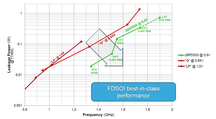
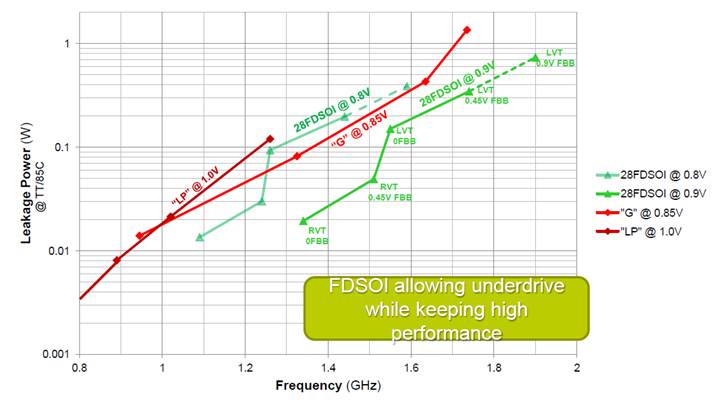
- FDSOI is faster than Bulk. If you take some time to decrypt the above picture, you will see that, for the same power budget, an ARM processor will reach slightly above 1.2 GHz on 28LP, 1.4 GHz on 28G and almost 1.6 GHz on 28FDSOI technology.

- FDSOI is cooler than Bulk. If you want your processor to consume as low power as possible, but still exhibit good performance, reaching for example 1.5 GHz, you will compare 28FDSOI @ 0.9V with 28G @ 0.85V (28LP is already “out”) and see that there is almost one order of magnitude in term of leakage power.
So, FDSOI is clearly an attractive technology, especially for wireless or multimedia AP, as it allows minimizing drastically the power budget (by almost an order of magnitude for the leakage power), or increasing the processor core frequency. In fact, using FDSOI is equivalent to design on one technology node back (28nm instead of 20nm), and benefit from lower mask cost and process complexity.
As I told you before, Semiwiki readers are pretty smart, and I have extracted two comments:
“Silicon-proven IP is prerequisite to the success of any technology. So, ST needs close collaboration with fabless companies, or maybe even opening up some of their designs or at least their experiment in designing with FDSOI to other parties.”
“One of the main pre-requisite for success of FD-SOI or FinFET will be availability of IPs. Most of the cases the selection of foundry, even process nodes depend on the availability of silicon proven IP.”
Because STMicroelectronics is a chip maker, they know how important it is to have the right IP port-folio available for SoC design on FDSOI technology. They have managed IP migration, to support their own SoC design, and propose the following approach, extracted from the White Paper “Planar fully depleted silicon technology to design competitive SOC at 28nm and beyond’:
At SOC level, migrating an existing design from bulk to planar FD represents an effort comparable to half-node migration, for example from 45nm to 40nm. In other words, it brings very worthwhile benefits at reasonable efforts. A typical approach could be:
- CPU and GPU: the main objective is maximum peak performance and the design is re-worked, making the most of FBB;
- Other SOC blocks: the main objective is power savings, by reaching the target operating frequencies at lower Vdd; there is no change to block design, Timing Analysis is re-run and ECO (Engineering Change Order) is performed to fix violations if needed.
- Other IP such as IOs and PHY blocks are swapped for their planar FD counterpart.
As far as I am concerned, I think that the availability of the right IP on FD-SOI will be very important for the adoption of this technology. STM seems to be on line with this position, as Giorgio Cesana, Director of Marketing and Communication, STM, will present at IPSOC Grenoble, on November 6[SUP]th[/SUP]a paper titled: “FD-SOI Technology for Efficient SoC: IP Development examples”. I definitely plan to attend, and I will give you a feedback about it!
From Eric Esteve from IPNEST
More Articles by Eric Esteve …..
lang: en_US
Share this post via:


Musk’s Orbital Compute Vision: TERAFAB and the End of the Terrestrial Data Center