A vexing chip design issue is how to achieve (or improve) performance and power dissipation targets, allowing for a wide range of manufacturing process variation (P) and dynamic operation voltage and temperature fluctuations (VT). One design method is to analyze the operation across a set of PVT corners, and ensure sufficient design margin across this multi-dimensional space. Another approach is to dynamically alter the applied voltages (globally, or in a local domain), based on sensing the changing behavior of a reference circuit.
The introduction of fully-depleted silicon-on-insulator (FD-SOI) device technology has led to a resurgence in the opportunities for incorporating circuitry to adaptively modify the device bias conditions, to compensate for PVT tolerances. This interest is further advanced by the goals of many applications to operate over a wider temperature range, and especially, to operate at a reduced VDD supply voltage to minimize power dissipation.
At the recent International Solid State Circuits Conference (ISSCC 2021), as part of a collaboration with GLOBALFOUNDRIES and CEA-Leti, Dolphin Design presented an update on their IP offering to provide adaptive body bias (ABB) to FD-SOI devices to compensate for PVT variation and optimize power/performance, with minimal overhead. [1] This article provides some of the highlights of their presentation.
Background
For decades, designers have implemented methods to modify circuit performance based on real-time sensor feedback.
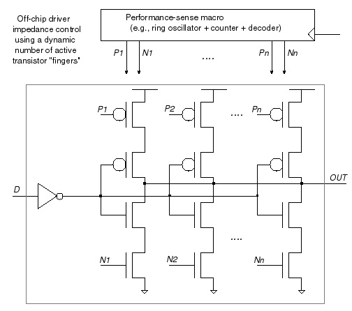
One of the first techniques addressed the issue of PVT variation on the output current of off-chip driver circuits – a critical design parameter is to maintain an impedance match to the package and printed circuit board traces to minimize signal reflections. A performance-sense ring oscillator (odd inverter chain) delay was used as a real-time PVT measurement. The frequency of the PSRO was compared to a reference, and additional parallel devices were added/disabled to the off-chip driver pullup and pulldown device stacks – see the figure below. [2]
Another method that was commonly used to adjust the operational behavior was to dynamically alter the substrate bias applied to the design. Recall that the threshold voltage of the FET is a function of the source-to-substrate voltage difference across the semiconductor p-n junction – by modulating the substrate bias, the Vt would be adjusted and the variation in circuit performance improved. (As the magnitude of the junction reverse bias increases, Vt increases as well; reducing the reverse bias reduces the Vt magnitude and improves performance. A small bulk forward bias is also possible to further improve performance – e.g., ~100-200mV – without excessive junction diode current.)
In the very early nMOS processes, the p-type substrate was common to all devices (enhancement-mode and depletion-mode nFETs). A charge pump circuit on the die generated a negative Vsub, periodically pulling capacitive-coupled current out of the substrate. By sensing a reference device Vt real-time, the duration and/or magnitude of this charge pump current could be modified. [3] For a 5V nMOS process, with a nominal Vsub = -3V, there was plenty of range available to modify the back bias.
The transition to CMOS processes introduced the need to consider both the p-substrate and n-well as potential body bias nodes. Designers developed a strategy for inserting p-sub and n-well taps throughout the die to connect to bias supplies, separate from the VDD and GND rails connected to the circuitry.
With the ongoing Dennard CMOS scaling associated with Moore’s Law, body bias techniques were less viable. The additional reverse-bias electric field across the junction is a breakdown issue at scaled dimensions. As a result, Vsub typically became the same rail connection as GND, and Vnwell was the same rail as VDD. If distinct substrate bias control to the devices was required, CMOS processes were extended to include a triple-well option – see the figure below.
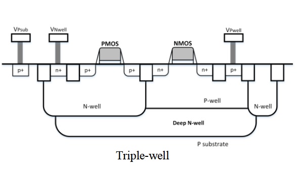
An additional p-well inside a deep n-well inside the p-substrate allowed unique reverse-bias voltages to be applied to the n-well (pMOS) and local p-well (nMOS) devices.
Rather than using body bias, designers increasingly looked to adjust the VDD power supply for PVT compensation, a technique commonly denoted as dynamic voltage, frequency scaling (DVFS). Parenthetically, the use of DVFS methods was expanded beyond adaptive compensation for a target frequency to also provide boost modes of higher frequency operation at higher supplies, as well as a variety of power management states at reduced supply values. (And, the market for PMICs exploded, as well.)
The introduction of SOI device technology – and FD-SOI, in particular – changed the landscape for adaptive body bias techniques. A FD-SOI cross-section is shown in the figure below.
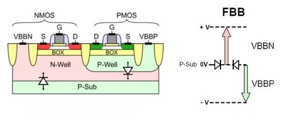
Note the use of the triple-well fabrication technique, allowing a unique back bias to be independently applied to nMOS and pMOS devices. Also, note the devices shown above are different than the conventional CMOS process technology. The nMOS above is situated above an n-well, while the pMOS is situated above a p-well – this topology would be reversed in a typical CMOS process. This unique FD-SOI process option is used to implement low Vt devices.
The presence of the thin isolating buried dielectric layer (BOX) below the device channel re-introduces the option of applying a p-well and n-well bias. This technique involves etching the well contacts through the (thin) silicon channel and dielectric layers of the FD-SOI device.
The p-n junction breakdown electric field issues of scaled CMOS are eliminated – the allowable electric field across the BOX dielectric is greater.
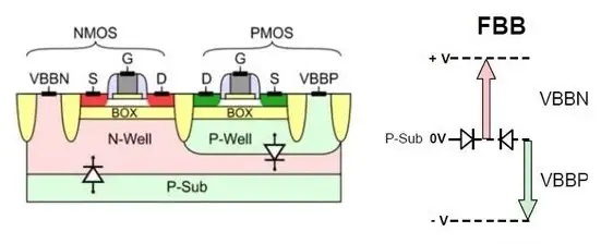
The FD-SOI device topology shown above offers the opportunity to apply an effective forward bias to the body, reducing the threshold voltage magnitude and boosting performance. (In a conventional CMOS process, the nMOS device would be subjected to a reverse bias relative to the channel, applied to the p-substrate.)
The BOX dielectric isolates the channel region – there is no source/drain-to-substrate diode junction. Note that bias restrictions remain for the p-n junctions of the device wells below the BOX.
Although the forward body bias technique increases the device leakage current, the supply voltage required to meet the target frequency can be reduced, with an overall power savings – more on that shortly.
Thus, there is renewed emphasis on the integration of ABB circuitry for FD-SOI designs, to compensate for PVT variations and/or optimize the operational frequency and power dissipation.
Dolphin ABB IP
A block diagram of the ABB IP is shown below.
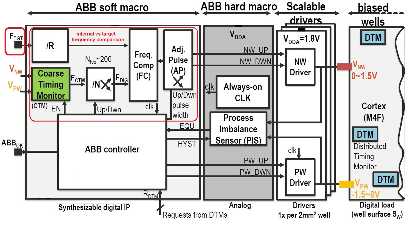
A primary input to the IP is the target operational frequency for the controlled domain, Ftarget. (For the Arm Cortex M4F core testcase design, the Ftarget was in the range ~10MHz – 1.5GHz.)
A coarse timing lock to this target is provided by a frequency-lock loop (FLL) circuit, comprised of a (digital) frequency comparator that generates adjust pulses to modulate the currents into n-well and p-well. Specifically, the lock is based on two separate divider ratios, R and N, one for Ftarget and one for an internally generated clock, Finternal. Lock is achieved when (Ftarget/R) = (Finternal/N).
The internally-generated clock reference for the frequency-lock loop in the ABB controller also includes PVT sense circuitry, to reduce the variation in the ring-oscillator frequency.
When the coarse monitor-based FLL is locked, the dynamic fine-grain adaptive bias is enabled. The detailed adjust to the n-well and p-well current drivers uses feedback from timing monitors distributed throughout the design block to be controlled by the ABB IP.
As voltage(s) and temperature(s) within the block fluctuate, the monitor(s) signal the ABB controller to increment/decrement the divider ratio “N” to adjust the well current drivers, maintaining the lock to the target frequency, as illustrated in the figure below.

The implementation of the ABB IP is all-digital for the FLL control and feedback, and the distributed timing monitors in the block. The exception is the charge pump circuitry that provides the p-well and n-well currents – in the Dolphin ABB IP, a VDDA=1.8V supply is used, the same supply as provided to the I/O cells. This enables a range of back bias voltage values from the charge pump.
Testsite and Measurement Results
The Dolphin team incorporated the ABB IP with an Arm Cortex M4F core, in a 22nm FD-SOI testsite fabricated at GLOBALFOUNDRIES – see the micrograph below, with the related specs.
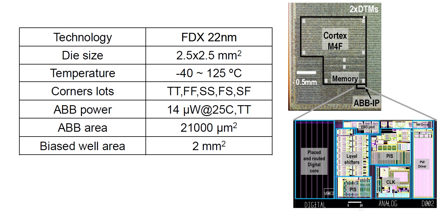
For this testsite, Dolphin chose to implement the Arm core using LVT-based cells and forward-body bias, with the device cross-section shown above. The focus of this experiment was to achieve the target frequency at a low core supply voltage, thereby reducing overall power dissipation. The available forward body bias values were:
- LVT nMOS – Vnw: 0V to 1.5V (FBB)
- LVT pMOS – Vpw: 0V to -1.5V (FBB)
Measurement data examples are shown below, illustrating how the Vnw and Vpw bias voltage varies with sweeps in temperature and supply voltage, to maintain lock to the target frequency.
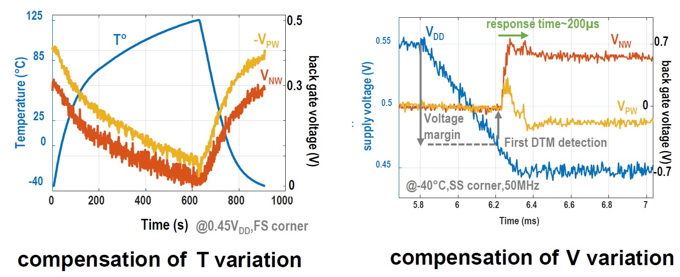
Note that the independent current sources for the p-well and n-well imply that these bias voltages may be asymmetric.
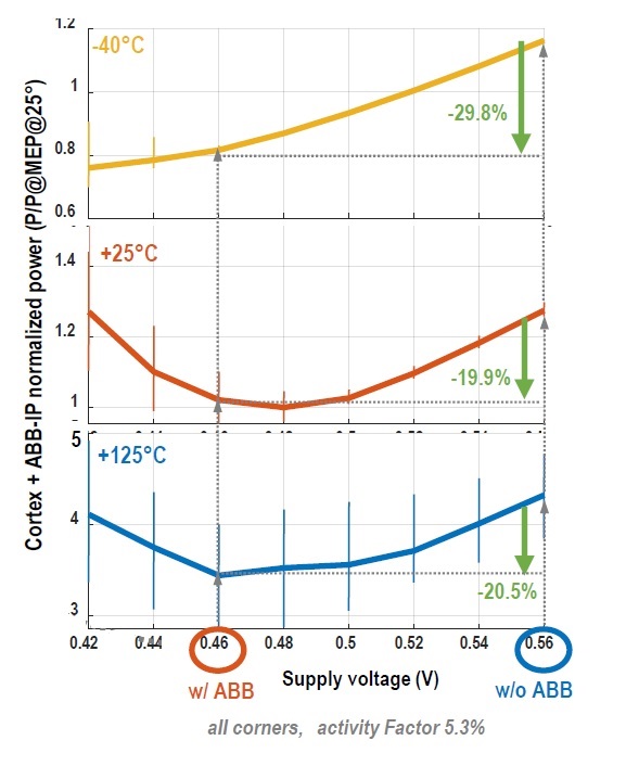
Of critical importance is the ability to use ABB to reduce the (nominal) core supply voltage, while maintaining the target frequency specification. For this design testsite, the use of LVT cells and ABB with forward bias enabled a reduction of ~100mV in the supply, while still meeting the target frequency – e.g., from 0.55V to 0.45V. This results in a ~20% overall power savings, as illustrated below (shown across three temperature corners, including both the power dissipation of the Arm core and the additional ABB IP).
Summary
FD-SOI technology has reinvigorated the interest in using adaptive body bias techniques for maintaining the operational target frequency over PVT variations. Both reverse-body bias (RBB) and forward-body bias (FBB) techniques can be applied, to RVT and LVT device configurations. At the recent ISSCC, Dolphin Design demonstrated how their ABB IP integrated with a core block can utilize FBB to achieve and dynamically maintain a target frequency. This technique relaxes the corner-based design margin constraints that typically define the supply voltage – a low supply can be selected, with the corresponding power savings.
Here is a link with additional information on adaptive body bias techniques in FD-SOI – link.
-chipguy
References
[1] Moursy, Y., et al., “A 0.021mm**2 PVT-Aware Digital-Flow-Compatible Adaptive Back-Biasing Regulator with Scalable Drivers Achieving 450% Frequency Boosting and 30% Power Reduction in 22nm FDSOI Technology”, ISSCC 2021, paper 35.2.
[2] Dillinger, T., VLSI Design Methodology Development, Prentice-Hall, 2019.
[3] US Patent # US-4553047, “Regulator for Substrate Voltage Generator”.
Share this post via:


Musk’s Orbital Compute Vision: TERAFAB and the End of the Terrestrial Data Center