Perforce recently held their virtual Embedded DevOps Summit. There was a lot of great presentations across many disciplines. Of particular interest to me, and likely to the SemiWiki readership as well, was a presentation by Warren Savage entitled Secure Collaboration on a Cloud-based Chip Design Environment. I’ll provide a quick overview of the event and then I’ll dive into Warren’s presentation to illuminate the Perforce Embedded DevOps Summit 2021 and the path to secure collaboration on the cloud.
I’ve been to A LOT of virtual events this past year. I’m sure you have as well. After attending so many you start to get a sense of what works best. Live presentations and a robust way to interact with the speakers are two elements I find appealing. The Perforce DevOps Summit had both. The presentations were live, and each session had a live moderator to keep things moving. This makes the event a lot more interesting in my experience. Interaction with the speakers was done through Slack, a robust and reliable platform. All good.

Back to secure collaboration on the cloud. I’ve known the presenter, Warren Savage for a long time. Warren has a very relaxed and effective style. He seems to be able to explain any complex topic in a way that everyone can understand. Warren is a Silicon Valley veteran who hails from places like Fairchild, Tandem Computers and Synopsys. In 2004 he founded IPextreme with the goal of simplifying IP access. Silvaco acquired the company on 2016 and Warren has now been recruited by DARPA to work on cybersecurity.
The organization he’s working with is called ARLIS (Applied Research Laboratory for Intelligence and Security). The organization has a broad charter in research and development for artificial intelligence, information engineering and human systems. Warren’s talk had two parts – one that outlined the significant security risks that exist in the devices and networks we use every day and one that detailed the work DARPA is doing with Perforce to address these risks. Let’s take a look at both parts.
Vulnerabilities – Be Worried
Warren began with an overview of the incredibly connected world around us – how we got there. Most of us know this story quite well, so let’s skip to what’s wrong with it. If we look at all the interconnected devices around us, they communicate with the cloud and with each other. IoT is a good example. The issue with this massive network of devices is the uneven security that exists across the spectrum. Simple IoT devices can have weak security. Warren used the digital picture frame you give your grandmother so you can stream photos of her grandchildren to her as an example. This sounds innocent enough, but it turns out these devices present a meaningful attack vector.
Warren recounted the incident in 2016 when a denial-of-service attack on a major DNS server took the internet down on the east coast of the US and Europe for about a day. This attack was accomplished with a weapon called the Mirai botnet. Essentially a massive network of vulnerable devices (like that picture frame) all co-opted to perform a specific attack protocol. These botnets can be assembled in a hierarchical fashion, creating formidable processing power. The recent SolarWinds hack is another example of how large the scope of these efforts can be.
DARPA has created an Attack Surface Reference Model that catalogs the various methods to misappropriate chip technology. There are four primary vectors:
- Side channel: extraction of sensitive data by observing external chip characteristics, such as power consumption or network traffic
- Reverse engineering: extraction of algorithms and design details from illegally obtained representations
- Malicious hardware: insertion of secretly triggered disruptive functions in the device
- Supply chain: cloning, counterfeiting or re-marking devices
It turns out the semiconductor supply chain represents an enormous attack surface, some of the opportunities are detailed in the figure below.

The Work Ahead – Be Less Worried
Warren described a rather ambitious program underway at DARPA to address these threats. Called Automatic Implementation of Secure Silicon (AISS), the goal is to embed security capabilities into the design flow. New tools and new IP will play a part. There are already approaches to address some of the threats mentioned. EDA tools can add additional logic to a chip that modifies its behavior. Only by entering a key can the chip’s original function be restored. This basically makes reverse engineering very difficult. The program’s goal is to add a fourth parameter to the familiar power, performance and area metrics (PPA) for security.
Warren went into some advanced work using blockchain technology to track the chain of custody of material in the semiconductor supply chain. This will help to close many attack surfaces. Back to AISS. There is a mandate that this system must operate entirely in the cloud. There is a lot work going on to host a familiar-looking, easy-to-use design flow in the cloud to deliver new security technology.
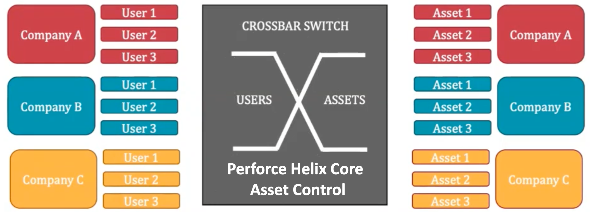
This design flow is where Perforce technology is used. A key goal of the system is to facilitate controlled access of assets from multiple companies who participate in a design project. Certain assets need access by specific users in multiple companies. Something like a crossbar switch is required to implement a system like this, and the Helix Core from Perforce is an excellent match for this need. The architecture of the system is shown below.

The complete agenda of the Embedded DevOps Summit 2021 can be found here. I suspect there will be an opportunity to watch replays of the event. Keep watching here to get more information on the Perforce Embedded DevOps Summit 2021 and the path to secure collaboration on the cloud.
The views, thoughts, and opinions expressed in this blog belong solely to the author, and not to the author’s employer, organization, committee or any other group or individual.
Also Read:
Single HW/SW Bill of Material (BoM) Benefits System Development
Share this post via:


Comments
There are no comments yet.
You must register or log in to view/post comments.