The last session I attended at DesignCon 2020 wasn’t a session at all. Rather it was an interactive discussion with Todd Westerhoff, product manager for electronic board systems at Mentor Graphics. Todd made some observations about the way high-performance PCBs are designed today and perhaps the way they should be designed. Todd has a long career in EDA and high-speed design, including a stint managing high-speed systems design at Cisco, so I was ready to listen carefully. As an aside, we spent some time discussing the birth of EDA and what it all (might) mean. That’s a story for another day.
Let’s start with the fundamental premise of Todd’s discussion – experts can 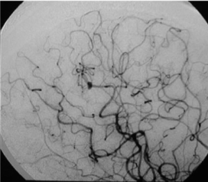 instantly spot problems invisible to others. The experts in this case are the signal integrity design experts that we all wish we had more of. To make this point, Todd shared the image on the right. It’s a brain scan, and it clearly shows a problem. Do you see it? This would require a different kind of expert. If you think you know what’s happening in this picture, put it aside for now. We’ll discuss the answer later.
So, what’s the core issue we’re discussing? The following diagram that details the health of hardware design projects sums it up.
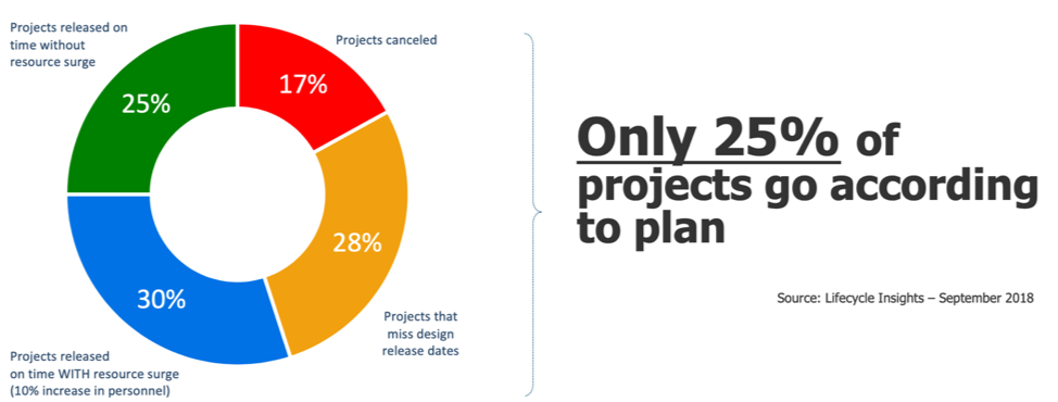
25% simply isn’t a good hit rate. What can be done about this? Ideas around this goal occupied the balance of my discussions with Todd. High performance PCB design is hard – signal integrity issues will kill your design if you’re not careful. There’s nothing really new in this statement, but let’s take a closer look at how the difficulty of these designs is manifested in the design flow.
In any given high-speed, high-performance PCB design, there are clearly areas of concern from a signal integrity perspective. The areas where crosstalk and coupling are likely to be an issue get close attention from the SI experts. There are a lot of tools and a lot of complexity in this part of the design process. The figure below is an example of how things stack up for a SerDes channel.
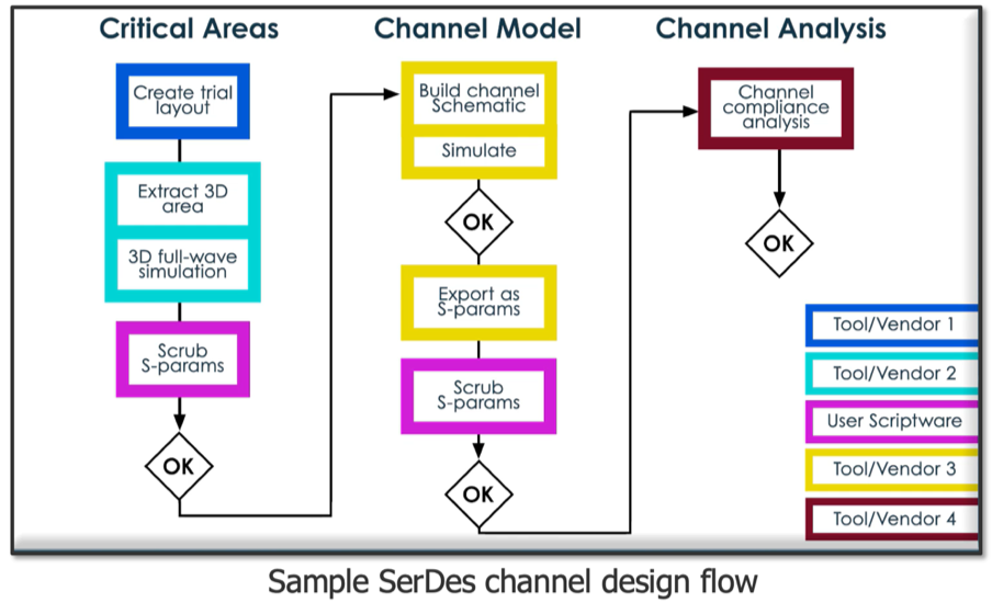
This is the risky part of the design, but this is NOT where the typical killer defect emerges. There are way too many expert eyeballs looking at this part for that to happen. Rather, it’s the rest of the design, the parts that go through traditional design reviews, that usually get you. The “small stuff” as Todd would say. There are always SI hotspots that are aren’t noticed and so these parts of the design get a level of scrutiny that is insufficient to see and fix the problem.
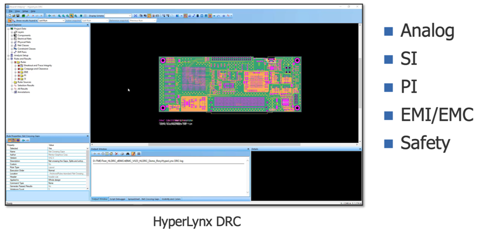
Todd posed the following solution: What if you could create an automated design review checking system? One that gives designers the capability to run first-order analysis themselves. One that automates and integrates analysis of things like crosstalk and DRC into existing design processes and one that can run overnight, providing the design team a “heat map” of issues to look at as a result of yesterday’s work. This started to make a lot of sense to me.
It turns out Mentor is beginning to work with customers to deploy such an automated design review system. The figure below shows what it looks like. Note the Mentor HyperLynx DRC tool is mentioned. It turns out Mentor has tools to cover the entire automated design review flow. Watch this work from Mentor, I think it has great promise to get that 25% hit rate much higher.
And by the way, regarding that brain scan, the problem area highlighted is an 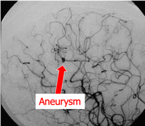 aneurysm. This is a real case, where the problem was identified early and repaired. If you got this right, there might be other job opportunities for you in addition to impossible chip/system design.


Comments
There are no comments yet.
You must register or log in to view/post comments.