Physical IC design is a time consuming and error prone process that begs for automation in the form of clever EDA tools that understand the inter-relationships between logic synthesis, IC layout, test and sign-off analysis. There’s even an annual conference called ISPD – International Symposium on Physical Design, and this year it was held in San Francisco, April 14-17. For the keynote speaker this year they invited Shankar Krishnamoorthy from Synopsys to talk about, “Fusion: The Dawn of the Hyper Convergence Era in EDA“. I was able to review his presentation to better understand the challenges and EDA approach that Synopsys has undertaken.
Before I delve into EDA tools, let me first take a step back and review what’s happened in the datacenter recently, where three mostly separate technologies have morphed into a single, more optimized system (aka hyperconvergence):
- Computation
- Storage
- Networking
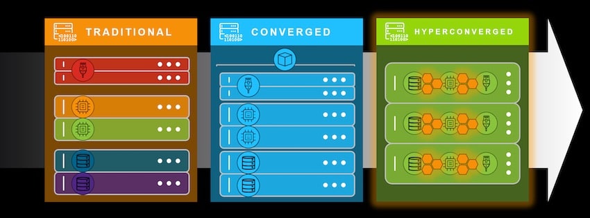
So a hyper-converged infrastructure (HCI) uses software and virtualized elements running on commercial, off-the-shelf servers to improve performance and enable easier scaling. In the traditional datacenter server the networking could come from Cisco, the compute by HP and storage by EMC, but the setup and maintenance was complex, a bit inefficient and scaling was brute force.
By the 2010’s we saw datacenter servers take a converged approach where either Simplivity and HP partnered, or EMC and Dell partnered, so it was easier to manage than the traditional data center but still had issues with limited capabilities and reliability.
Since the mid 2010s we now see the emergence a hyperconverged datacenters with vendors like Nutanix that have fused together the once separate components of storage, compute, networking and virtualization.
I’ve been an EDA tool user since 1978 and blogging about EDA tools for over 10 years, so I’ve seen many generations of tools being offered. Through the 1990s we saw many CAD groups combining multiple point tools into a traditional flow for nodes down to 90nm, as shown below. Sure, you could mix and match the best tool for each task, yet there would always be iterations to reach closure.
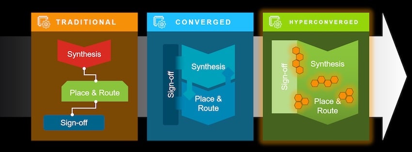
The converged approach has been in use since 2000 and used on IC implementation down to 7nm, with EDA vendors typically providing more integration and links between the tools. Benefits with a converged approach are more coherency, and an improvement in predictability, but the sheer size of IC designs and unprecedented complexity due to relentlessly advancing Moore’s Law have made even this methodology unviable.
Going from RTL code to signoff while meeting the QoR and productivity targets is a much bigger task at 7nm and below, so creating an EDA tool flow to meet this challenge could take a couple of approaches: Loose coupling between multiple engines using separate data models, or a single data model with common engines.
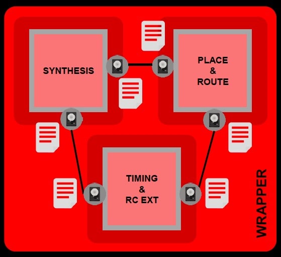
Loose coupling between engines
With a loose coupling approach between engines there’s still an issue meeting PPA (Power, Performance, Area) and convergence, because you don’t always get a predictable improvement over time, and the runtimes are lengthened because there are still iterative recipes being used.
The hyperconverged “Fusion“ approach is distinguished by a single data model, single user cockpit and common interleaved engines:
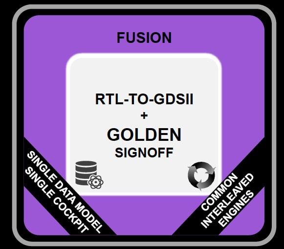
The promise of this approach is a quicker convergence to optimal PPA. Just think about how an end-to-end physical implementation system unified on a single data model and using common synthesis, place-and-route and signoff engines could enable seamless optimization throughout the flow for superior QoR and signoff predictability:
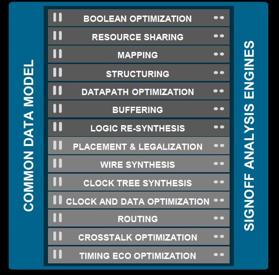
OK, the theory of hyperconverged EDA tools sounds interesting, but what about actual results? One IC design with 2.5M instances and 5 power domains using a 16nm process was run in both converged and hyperconverged tools, showing the following improvements:
- 2.4X faster full-flow turnaround time
- 46% better timing
- 11% less area
Engineers love data, so here are some more results using the hyperconverged approach on multi-million instance designs at 16nm and 7nm process nodes:
- Mobile CPU
- 10% Total Negative Slack (TNS) improvement
- 10% Leakage improvement
- 3% Smaller area
- Automotive IC
- 28% TNS improvement
- 13% Smaller area
- High performance server SoC
- 56% Leakage reductions
- 41% Faster runtime
- 10% Smaller area
So this new hyperconverged Fusion approach from Synopsys uses many common optimization technologies throughout the flow to concurrently optimize across multiple metrics, including timing, power, IR drop, area and congestion. For instance, by using an integrated IR analysis engine in the flow it can resolve IR violations without impacting timing closure, look at one comparison versus the baseline flow:
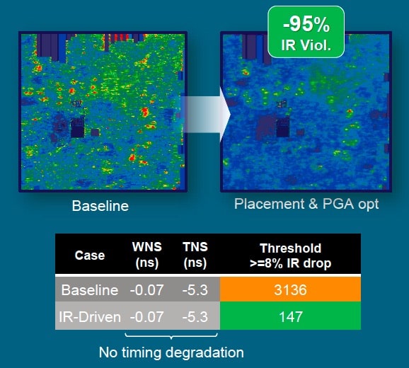
The baseline flow had 3,136 IR violations where the threshold was >=8% IR drop, while the Fusion flow had just 137 IR violations, that’s a whopping 95% reduction with the newer approach.
Summary
If you use the same EDA methodology from a 28nm flow on a 7nm or 5nm SoC, then there are going to be some big surprises as you iterate and attempt to reach an acceptable PPA value within the time budget allotted. Change with the times and consider the hyperconverged approach being offered by Synopsys in Fusion, the early numbers looked promising to me.


Comments
One Reply to “IC Implementation Improved by Hyperconvergence of Tools”
You must register or log in to view/post comments.