By offering low-power PCI Express PHY solution for mobile application! To make it clear, we are not talking about Mobile Express (M-PCIe), but clearly about PCI Express protocol, including a PCIe Controller and a PCIe PHY. Initially developed to support internal connection between the CPU and the GPU in a PC, the technology has been incredibly successful and pervasive. When a new PCIe generation is released, like gen-3 at the end of 2010, the early adopters are searching for maximum performance, like in server, networking or storage applications. High performance associated with high power consumption, but the power is not the primary issue for such applications. But low power is definitely a key target for any mobile, battery powered device. By launching a PCIe gen-3 PHY IP specifically designed for low power behavior, offering industry smallest active power (as low as 50 mW per lane at 8 GT/s) as well as standby power (less than 10 mW per lane), Synopsys clearly target mobile systems like Ultrabook or Tablet.

PPA: Power, Performance and Area are the IP’s keywords. Let’s have a look at this PHY performance first. PCI-SIG has defined PCIe channel performance requirements for PCIe 3.1 technology. The state of art in mixed-signal design implies using these techniques to enhance signal integrity across high loss and bumpy channels and comply with the specification:
- multi-phase-locked loops (MPLLs),
- Feed Forward Equalization (FFE),
- Continuous Time Linear Equalization (CTLE),
- programmable Decision Feedback Equalization (DFE)
This low power PCIe 3.1 PHY is said to meet the specification and also provides flexibility and scalability for high-speed SoCs by offering separate Refclk Independent SSC (SRIS), reference clock forwarding and PCI Express architecture aggregation and bifurcation. No doubt that this is a fully compliant PCIe 3.1 PHY, exhibiting the same performance than any other IP. But which makes it unique is power efficiency, let’s look at the active power consumption characteristic: 5 mW per lane and per GT/s.
This PHY is supporting supply under drive, a novel transmitter design and equalization bypass schemes. Designing PCIe PHY to support a mobile application, typically SSD card to replace HDD for internal storage, means that the PCIe bus will not drive any long interconnect like a backplane in networking, but rather a few cm long lane(s) to connect the internal SSD with the CPU. That’s why it’s possible to bypass equalization for example, and severely reduce poser consumption. Active power consumption is important, but for a mobile device the leakage power is even more important, forcing you to charge the battery even if you don’t intensively use your device!

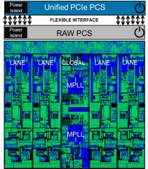
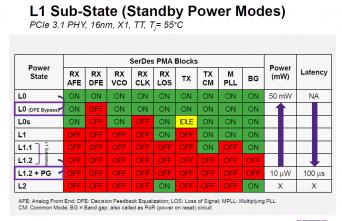
The PCI Express specification defines various power states, L0, L1 sub-states and L2 in order to frame different power conditions. It’s important to keep in mind that, if you can design as you wish to lower the power, you will have to comply with one firm requirement: the 100 ms maximum latency or time to come back to a fully working state. You can see on the above table how the various functions are managed (ON, OFF or IDLE) to comply with the various power states. To be able to put OFF a certain function within a design, Synopsys had to use well-known (at least for mobile SoC designers), power gating, power islands and retention cells techniques. Because a PCI Express is made of a PHY and a Controller, the power gating techniques have been exercise both on the Controller and the PHY raw PCS as well as protocol PCS (both in RTL) via Unified Power Format (UPF). In fine, the power savings in the controller with the L1 sub-states and power gating have given up to 95% reduce current.

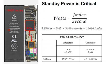
Just take an example with this mobile device breakdown. You can see the battery specification of 5.45 Whr, or 19620 Joules. The “usual” PCIe IP targeting enterprise segment exhibit around standby power of 2 mW, as no specific care has been taken to reduce it. This translates into 9% of the 10 days battery life… and this is not the only semiconductor device integrated into this application! When designing for low standby power, you come down to 0.02% of the 10 days battery life.
One of the PPA is missing: Area. When we speak about area, we think about cost (a direct impact of the die area). This IP has been designed in such a way that it’s not only the industry’s lowest power, but also the unique PCIe 3.1 PHY IP accepting wire bonding. Wire bond is easily translated into cheap package!
From Eric Esteve from IPNEST
Share this post via:


Comments
There are no comments yet.
You must register or log in to view/post comments.