
In a rapidly evolving semiconductor landscape, where AI demands unprecedented computational power and efficiency, Synopsys has deepened its partnership with TSMC to pioneer advancements in AI-driven designs and multi-die systems. Announced during the TSMC OIP Ecosystem Summit last week, this collaboration leverages Synopsys’ EDA tools and IP solutions alongside TSMC’s cutting-edge processes and packaging technologies. The result? Accelerated innovation that empowers chip designers to create high-performance, low-power multi-die architectures essential for next-generation AI applications, from data centers to edge devices, absolutely.

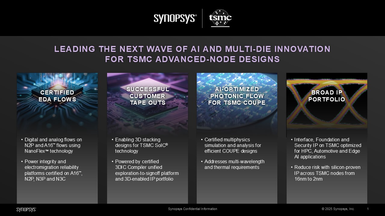
At the heart of this alliance is Synopsys’ commitment to enabling differentiated designs on TSMC’s advanced nodes. Certified digital and analog flows, integrated with Synopsys.ai, are now available for TSMC’s N2P and A16 processes, incorporating the innovative NanoFlex architecture. This setup not only boosts performance but also streamlines analog design migration, allowing engineers to scale chips efficiently while optimizing power consumption. For the A16 node, Synopsys has enhanced capabilities for Super Power Rail (SPR) designs, improving power distribution and thermal management in backside routing. Additionally, pattern-based pin access methodologies have been refined to deliver superior area efficiency. Looking ahead, the duo is already collaborating on flows for TSMC’s A14 process, with the first process design kit slated for release later in 2025.
")
Physical verification is equally robust, with Synopsys’ IC Validator certified for A16, supporting design rule checking (DRC) and layout versus schematic (LVS) verification. Its elastic architecture handles complex electrostatic discharge (ESD) rules on N2P with faster turnaround times, ensuring reliability in high-stakes AI systems.
A standout feature of the collaboration is the focus on 3D integration, addressing the limitations of traditional 2D scaling. Synopsys’ 3DIC Compiler platform, a unified exploration-to-signoff tool, supports TSMC’s SoIC-X technology for 3D stacking, as well as CoWoS packaging for silicon interposers and bridges. This has facilitated multiple customer tape-outs, demonstrating real-world success. The platform automates critical tasks like UCIe and HBM routing, through-silicon via (TSV) planning, bump alignment, and multi-die verification, slashing design cycles and enhancing productivity. In photonics, an AI-optimized flow for TSMC’s Compact Universal Photonic Engine (COUPE) tackles multi-wavelength operations and thermal challenges, boosting system performance in optical interconnects vital for AI data transfer.
Complementing these EDA advancements is Synopsys’ expansive IP portfolio, optimized for TSMC’s N2/N2P nodes to minimize power usage and integration risks. It includes high-performance interfaces like HBM4, 1.6T Ethernet, UCIe, PCIe 7.0, and UALink, alongside automotive-grade solutions for N5A and N3A processes. This suite—encompassing PHYs, embedded memories, logic libraries, programmable I/O, and non-volatile memory—ensures safety, security, and reliability across markets like automotive, IoT, and high-performance computing (HPC). For multi-die designs, specialized 3D-enabled IP further accelerates silicon success.
I spoke with Michael Buehler-Garcia, Senior Vice President at Synopsys at the event. He is a long time friend. He emphasized the partnership’s impact:
Our close collaboration with TSMC continues to empower engineering teams to achieve successful tape outs on the industry’s most advanced packaging and process technologies,” said Michael Buehler-Garcia, Senior Vice President at Synopsys. “With certified digital and analog EDA flows, 3DIC Compiler platform, and our comprehensive IP portfolio optimized for TSMC’s advanced technologies, Synopsys is enabling mutual customers to deliver differentiated multi-die and AI designs with enhanced performance, lower power, and accelerated time to market.”
Echoing this, Aveek Sarkar, Director of TSMC’s Ecosystem and Alliance Management Division, highlighted the ecosystem’s role:
“TSMC has been working closely with our long-standing Open Innovation Platform® (OIP) ecosystem partners like Synopsys to help customers achieve high quality-of-results and faster time-to-market for leading-edge SoC designs,”.
“With the ever-growing need for energy efficient and high-performance AI chips, the OIP ecosystem collaboration is crucial for providing our mutual customers with certified EDA tools, flows and high-quality IP to meet or exceed their design targets.”
Bottom Line: This synergy positions Synopsys and TSMC at the forefront of the AI revolution, where multi-die systems promise to overcome Moore’s Law bottlenecks by integrating heterogeneous dies for superior efficiency. As AI workloads explode, such innovations will reduce energy footprints in hyperscale data centers and enable smarter autonomous vehicles.
Also Read:
Synopsys Announces Expanding AI Capabilities and EDA AI Leadership
AI Everywhere in the Chip Lifecycle: Synopsys at AI Infra Summit 2025
Synopsys Collaborates with TSMC to Enable Advanced 2D and 3D Design Solutions
Share this post via:


Comments
There are no comments yet.
You must register or log in to view/post comments.