Listening to a webinar at your desk, in front of a PC screen will never replace a live presentation, but the lesson learned to time spent ratio can be incredibly higher than when traveling to a conference to listen several presentation. If you are interested by the approach taken by a complex DSP design team to overcome the various bottlenecks they have faced with, from synthesis to floor-plan and floor-plan to place and route (P&R), and want to understand how the team has selected the various Synopsys library cell and Memories, then this webinar is certainly for you:
“Optimizing DSP cores for Performance and Power with DesignWare Logic Libraries and Embedded Memories”
And you can register, and attend to the seminar right away, just go here

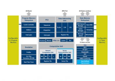
The above picture is the XC4210 diagram, one of the most complex DSP core from CEVA. XC4210 has a fully programmable DSP processor architecture, made of two vector processing units – each unit operates on 256-bit vector registers offering a powerful SIMD engine
- Up to 8 simultaneous instructions (8-Way VLIW)
- Efficient DSP support for non-vectorized data
- Efficient support for control and ANSI-C operations
Extremely powerful computation capabilities
- 64 16×16-bit MAC operations
- 64 arithmetic operations per cycle
- Over 400 16-bit operations in a cycle
The challenge is dual: this core has to be optimized both for Base Station implementation and for Mobile Handset application. Thus, the targets are very different:
- Base Station: the goal is Freq. > 1 Ghz, and Leakage < 1W
- Mobile Handset: the goal is Freq. > 400 Mhz, and Leakage as low as possible
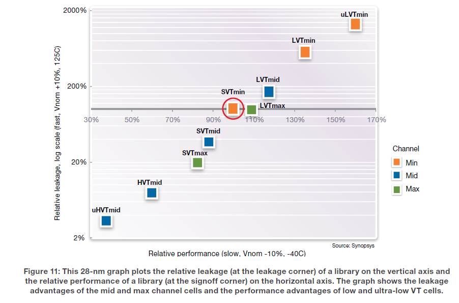
CEVA has used the Synopsys DesignWare TSMC 28 HPM standard cell library and memory compiler. If you take a look at the Power/Performance figure below, you realize that the cell selection possibilities are very wide, allowing optimization to be pushed to the limits, very low leakage for Handset application, very high performance for base station. In fact, CEVA claims to have reached 1.3 GHz, passing the target by 30% for the BS option!

Another challenge is the size of the on-chip memory, very large for a DSP core. Synopsys is offering Ultra High Density memories, offering 48% area saving (compared with the HD memory) along with a 33% better leakage, these memories have been developed to support CPU, GPU and DSP needs. You will find extremely useful information in this White Paper, “CPU, GPU and DSP Core Optimization for High Performance and Low Power”.
To know how CEVA has defined the Top Ten Bottlenecks: “Physical Design Challenges”
[LIST=1]
and even more important how the design team has manage to solve these bottlenecks, making the best use of Synopsys DesignWare 28HPM Library and design tools, you will have to listen the webinar. I also recommend listening to the questions, at the end of the webinar, all of these are relevant, and you will learn from the answer too!
From Eric Esteve from IPNEST
More Articles by Eric Esteve…..
lang: en_US
Share this post via:


Comments
There are no comments yet.
You must register or log in to view/post comments.