You may have noticed that I have been writing a lot more about analog design lately. This is no accident. Analog and custom blocks are increasingly important because of the critical role they play in enabling many classes of systems, such as automotive, networking, wireless, mobile, cloud, etc. Many of the SoCs needed for these markets are developed on advanced nodes, including FinFET. However, new design rules and other design complexities at these advanced nodes are making analog design more difficult and challenging.
Synopsys has a presentation at this year’s CICC that is titled “Has the Time for Analog Design Automation Finally Come?”, authored by Dave Reed and Avina Verma, which offers a close examination of methods for accelerating and improving how analog design is done. I had a chance to talk with them recently about their presentation. Automation of analog design is a laudable goal but has proven elusive. In part Dave and Avina attribute this to the fact that it’s more difficult for analog designers to provide a concise set of constraints to describe their design objectives. Asking analog engineers to create extensive text-based rules to drive the automation tools often results in just as much work as doing the physical design in the first place. They also say that tool designers need to ensure design tools match the way designers want to work.
Their point is that each stage of the design process has a preferred creation and editing method that any tools for automation should accommodate. They believe that encouraging iterative design is better than asking for a big up-front investment to specify the results. There are several key goals for an automation flow. Faster layout should be possible with automated correct device level placement and device level routing. Design closure requires consideration of resistance, capacitance and electromigration issues. Designers want to get early insight into parasitics. Lastly, design reuse, if done right, can offer a huge productivity boost.
As one example of using graphical methods, they point to the way Custom Compiler uses a symbolic graphical palette to pre-define placement patterns for devices. Along with this it provides a real-time display of the actual layout visible at the same time. Visual feedback is provided with color coded device visualizations and a centroid display. It also provides an easy way add dummies and guard rings.
Device routing automatically connects large device arrays while ensuring matched R/C routes. Interconnect with user-controlled hand-crafted quality is created with greater ease than with manual methods. Just as with placement, Custom Compiler provides a graphical palette of predefined routing patterns that designers can choose from. Users can drive the router by guiding it using their cursor on the layout. It comes with automatic connection cloning, pin taping and via generation. There is also interactive DRC and obstruction feedback.
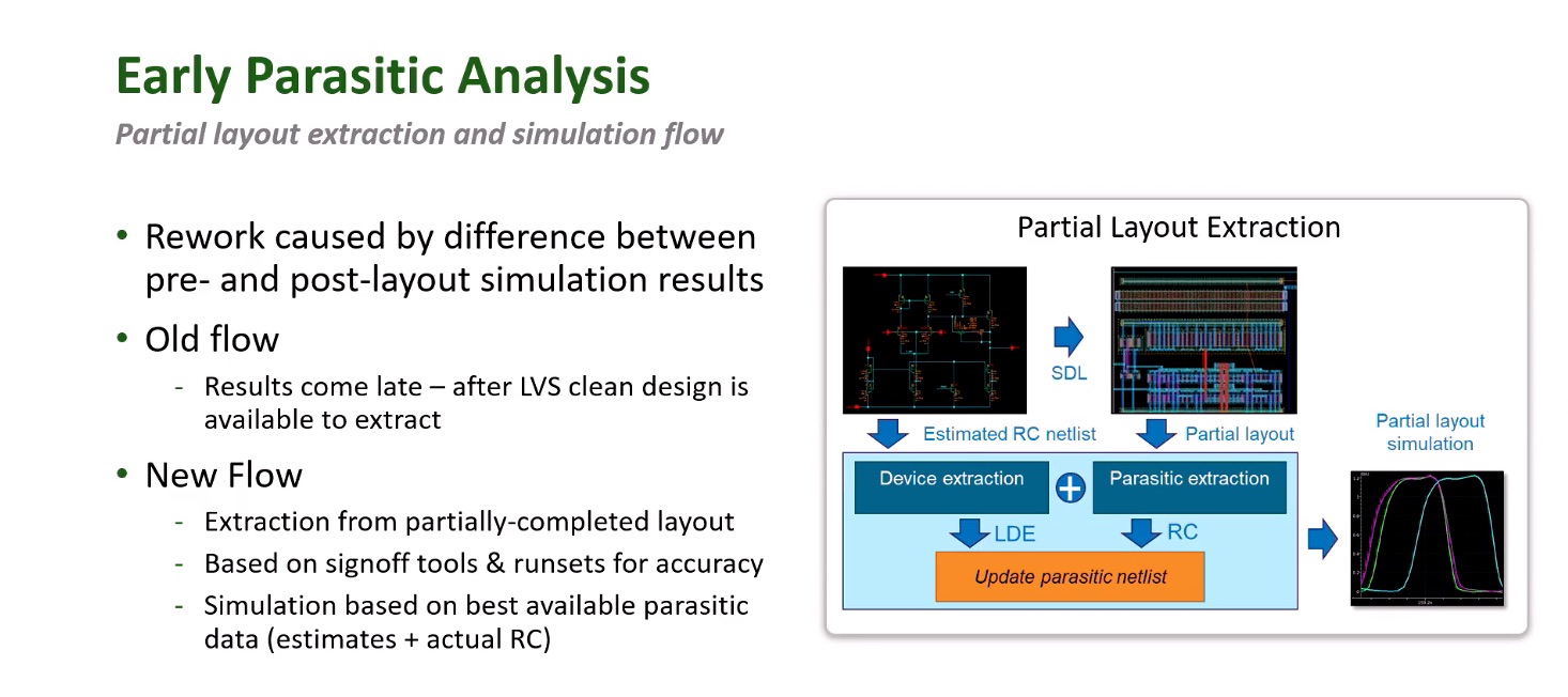
The key to moving from schematic to layout design closure is understanding layout parasitics quickly and accurately. Without this, rework effort can become considerable. Instead of having to wait until the design is LVS clean to run LPE and RC extraction, Custom Compiler’s schematic driven layout (SDL) flow gives layout engineers parasitics throughout the layout process. Before nets are routed, estimates are used. As nets are incrementally hooked up actual extracted parasitics are inserted for each one.

Even though the fully extracted design is not available until the end, enough information is available early in the process to help provide useful feedback. This is vastly preferable to waiting until the end of the layout process to get physical parasitic information. Synopsys has also been working on using machine learning to help improve prediction of parasitics for even better estimates earlier in the process.
I mentioned above that templates can be used to help drive placement. Dave and Avina talked about how existing designs can be mined to easily produce templates for device placement. Dave said that this is a favorite feature for a lot of users.
With the added complexity of advanced nodes, specifically with new complex design rules and the need to place or modify arrays of FinFET devices, automation of the analog layout process promises big gains in productivity and design quality. Dave and Avina argue that the time has finally come for the automation of analog designs. They understand that this will never be a “push the big red button” sort of thing but will instead be made up from numerous discrete capabilities that are easy for designers to integrate into their workflow.
More information is available through CICC in their educational session archives and also on the Synopsys web page for their custom design platform.
Also read:
Design to Layout Collaboration Mixed Signal
Synopsys Tutorial on Dependable System Design
Synopsys Announces FlexEDA for the Cloud!
Share this post via:


Comments
One Reply to “The Path Towards Automation of Analog Design”
You must register or log in to view/post comments.