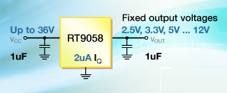
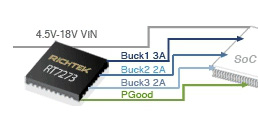
 With all the focus in design on SoCs in the latest sexy process (Hi-K Metal Gate! FinFETs!) it is easy to forget all the other chips that go into a system. When we say “system on a chip” there are actually very few systems that really get everything onto a single chip. One of the big areas that usually cannot go on the latest sexy process are the power management ICs that delivery very precise voltages to those SoCs starting from typically noisy power coming out of whatever plugs into the wall outlet, or from battery power that isn’t so noisy but that changes its characteristics as the battery runs down. One of the big design requirements for power management ICs is to do their work without wasting much of the power. In your smartphone, for example, wasted power shows up as a hotter phone to hold and shorter battery life, neither of which the end-user wants. It is especially important that the power management ICs consume only tiny amounts of power when the associated SoC is largely shutdown, as your smartphone is a lot of the time it is in your pocket.
These power management ICs are usually built in processes like 0.13um or 0.18um, which sound really outdated to the SoC designer but are actually the state-of-the-art processes for a lot of analog, mixed-signal and power designs.
Not surprisingly, the design process for a power IC is very different from that SoC. It is an important market: higher growth than the overall semiconductor market, very competitive, and with an increasing focus on power efficiency, delivering almost all the power taken in as input in whatever form is required as output, and consuming almost none in the power management IC itself.
One of the leaders in power management ICs is Richtek Technology. They have a large portfolio of parts that deliver innovative power management solutions that improve the performance of consumer electronics, computers, and communications equipment. Founded in 1998, the Company is headquartered in Taiwan with additional offices in Asia, the U.S., and Europe.
 K C Chang is the VP of Technology Development at Richtek. On October 3rd he will present a webinar, along with Andy Biddle of Synopsys, on some aspects of their design flow, their EDA tool selection criteria and some recent results. Andy will discuss the Galaxy Implementation Platform highlighting some of the recent capabilities that help power management IC designers bring highly efficient products to market earlier. They will present the key challenges and trends with latest power management integrated circuits and discuss recent EDA tool innovations to shorten development time and maximize quality of results.
If you are involved with the design of power management ICs then you should attend this webinar Power Management ICs – Efficient Design: A Richtek and Synopsys Perspective. The live webinar is on October 3rd at 10am Pacific Time. For more details and to register go here. The same link will work to view it after the event. It is scheduled to last 50 minutes plus Q&A.
Share this post via:


Comments
0 Replies to “Designing Power Management ICs”
You must register or log in to view/post comments.