This morning I spoke with Mahesh Tirupattur, Executive VP of Analog Bits about IC design challenges and using EDA tools to create high performance, mixed-signal semiconductor IP.
Q: What does Analog Bits offer?
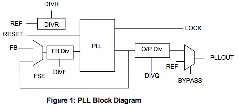
A: We do mixed-signal design, high-speed digital plus analog products like: PLL, DLL, SERDES/PMA, programmable I/O’s, specialized memories (SRAM/TCAM).

Q: Why did you join Analog Bits?
A: I’ve been with the company about 10 years now, background is CMOS circuit design, Sun, Virtual Silicon, EDA companies. I knew the founder for the past 25 years and admired his abilities. I wanted to help build the company.
Q: What are the analog IC design challenges that you face?
A: Traditional analog uses trailing edge process nodes, however we are using leading edge process nodes like 20nm. We’re even working on FinFET and FD-SOI nodes. We have to be looking out 3 years ahead in terms of process nodes, which can be un-finalized and still under development.
Q: What is your EDA tool flow for mixed-signal IC design?
A: Traditionally there was a circuit design team that tossed the design over the wall to layout design, then extraction back to analysis. Starting with 65nm we had more layout effects that dictated how a circuit could be designed, so it became almost layout-driven. Circuit designers really needed layout effects to start any circuit simulations.
At 28nm and 20nm the layout itself is very restricted by metalization factors, the wires are thinner and can be higher resistance, limiting the current. Issues like EM are limiting factors. Power is laid out first, then circuits are connected to the grid, a very different layout approach.
At 20nm the layout is almost like the old Gate Array with fixed orientations on devices.
On the electrical side we have to verify our semi IP across process variation using Monte Carlo simulations.
We do write Verilog-A models for some of our blocks that can be used in verification.
Q: How do you migrate previous semi IP into new nodes?
A: Migration of semi IP requires both layout and circuit effort. Moving from 90nm to 65nm took about 30% more effort. Going from 65nm to 45 nm the efforts went up 3X. Going to 20nm the efforts went up 6X because of new restrictions.
Mismatch is important for mixed-signal design performance, and we must make our designs tolerant of mismatch.
Q: Why did you choose Tanner EDA tools for analog IC design?
A: Firstly, we are a fast moving company and enjoy working with EDA vendors that are responsive. We like the PC-based tools from Tanner EDA, and we can easily upgrade our hardware to get higher performance.
Next, we don’t want to use a staff of CAD engineers and Tanner tools make it easy to get up to speed.
Pricing is attractive as we grow and need more licenses, we see good value.
Q: Which Tanner EDA tools do you have?
A: For IC layout it’s L-Edit, on schematic capture it’s S-Editfamily. Some RC extraction being used. For DRC we use Tanner initially, then final sign-off is Calibrefrom Mentor Graphics.

Q: What is your extraction tool?
A: We are using Star-RC extraction from Synopsys.
Q: How about circuit simulation?
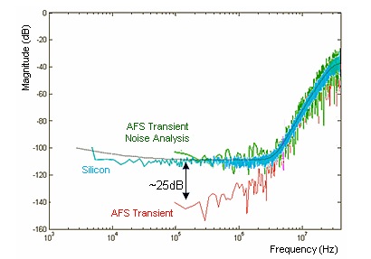
A: We use two different circuit simulators: FineSimfrom Synopsys, then noise analysis and phase jitter with Berkeley DA.

Q: What does the future for Analog Bits look like?
A: We want to grow at 30-40% year to year using our differentiated mixed-signal products. Serve our clients (Samsung, Sony, etc.) better than anyone else who need high performance semi IP like PLL and Serdes.
Further Reading
Analog Bits Continues to Drive Innovation for 0.25 micron to 20nm IC Designs Using Tanner EDA Schematic Capture and Layout Tools


Comments
0 Replies to “IC Design at Analog Bits”
You must register or log in to view/post comments.