Over the past 50 years in our industry, there have been three invariant principles:
- Moore’s Law drives the pace of Si technology scaling
- system memory utilizes MOS devices (for SRAM and DRAM)
- computation relies upon the “von Neumann” architecture
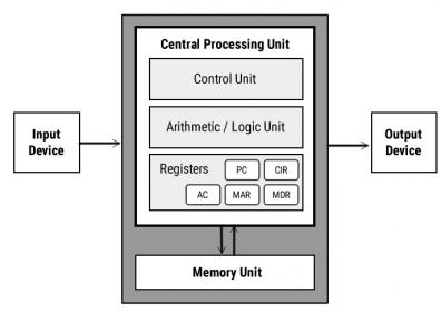
Figure 1. Block diagram of the von Neumann architecture
Today, all three tenets are being challenged – our industry is facing disruptive changes across the board.
Although Moore’s Law clearly still has a sustaining technology roadmap for another process node or two, the related costs are a driving force behind novel packaging technologies providing (heterogeneous) multi-die integration – some refer to this direction as “more than Moore”.
Traditional MOS system memory processes are being challenged by new approaches. Resistive RAM (ReRAM) and magneto-resistive RAM (MRAM) technologies utilize unique materials to alter the electrical (or magnetic) properties of a layer between two electrodes during a set/reset memory write cycle. The subsequent memory read cycle senses the electrical resistance through the layer to determine the bitcell value.
And, lastly, the von Neumann architecture for computation is being called into question, as to whether an alternative method could provide improved power/performance measures for certain applications – especially, AI machine learning tasks. The latency and power dissipation associated with frequent data/instruction memory access is an issue, especially for (massively) parallel and pipelined algorithms. An alternative architecture is needed for this class of computation to optimize power efficiency.
At the recent Silvaco Users Global event (SURGE), Blessy Alexander, Director of Design Technology at Applied Materials gave a compelling keynote presentation,“Role of Connective Materials to Systems for AI”. Her talk provided insights into how memory technology and computation architecture changes are needed to address the rapidly growing applications for neural network training and inference.
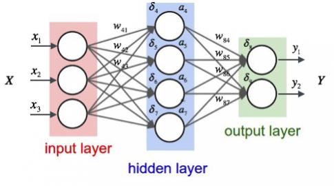
Figure 2. Neural network architecture
Recall that neural networks are comprised of multiple “layers” of nodes, where the computation at each node is commonly a weighted multiply-accumulate among the inputs to the node. An AI application would partition a data frame into neural network input values, and attempt to classify the data based upon the final results of the neural network computation. Each node in a layer consists of weighted multiply-add computations, whose total is refined by an activation function to provide the node output value. An initial training sequence is used to establish the weighting factors throughout the neural network layers, to achieve high classification accuracy on the reference dataset. In inference mode, the network is presented with runtime data to perform the classification evaluation.
The implementation of the NN using a von Neumann architecture requires accessing data and weight values from (traditional) memory, performing the computation in a (traditional) CPU, and storing the node results back in memory – an inefficient and highly dissipative approach.
Blessy highlighted the activity currently underway to realize neural networks using GPU hardware and/or custom chip designs – optimizations distinct from a von Neumann implementation. Then, she challenged our traditional thinking further, suggesting that the ReRAM technologies offer a very unique opportunity to represent the weight values, and thus, impact the entire NN computation.

Figure 3. Oxide-based Resistive RAM (OxRAM) — a cross section of the dielectric layer, illustrating ion/vacancy motion (From Perniola, “OXRAM Memories: A Disruptive Technology for Disruptive Designs”)
For example, consider the novel ReRAM technology known as Oxide-based resistive RAM, or OxRAM for short. For each bit cell, a unique dielectric material resides between two terminals. During a write cycle, the density of oxide vacancies is altered (i.e., dielectric locations where an oxygen atom has been removed), corresponding to a “set” or “reset” value. A read cycle measures the effective resistance of the cell, due to the motion of oxygen ions and vacancies (analogous to the motion of electrons and holes in a semiconductor).
The figures below illustrate the resistive characteristics of the OxRAM technology, with a depiction of a “1T-1R” bit cell in a traditional memory array configuration, with sense amplifiers used to detect each specific cell’s electrical properties during a read access.
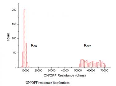
Figure 4. OxRAM cell resistance — Monte Carlo process simulation results (From Aziza, et al, “Oxide based resistive RAM: ON/OFF resistance analysis versus circuit variability”, IEEE 2014 International Symposium on Defect and Fault Tolerance in VLSI and Nanotechnology Systems.)
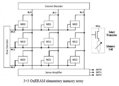
Figure 5. OxRAM based “1T 1R” memory configuration (From Aziza, et al.)
“But, what if the resistive characteristics of the ReRAM cell technology could be used to directly represent the weights of a neural network node?”, Blessy asked.
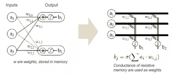
Figure 6. ReRAM cell resistance used as a neural network weight factor
The sense amplifiers would be replaced by an accumulation + activation function. As a result, the capacity and bandwidth constraints of the von Neumann approach would be greatly alleviated. A very interesting idea.
(In some regards, this would be similar to a binary-weighted summing digital-to-analog converter, I guess. Multiple ReRAM bit cells in parallel could be written to provide any of a large set of weights.)
The link between AMAT and Silvaco TCAD tools was the final part of Blessy’s presentation. New materials used in process technologies such as ReRAM require a close interaction among process development, physical characterization, model generation, and circuit simulation — part of the “Physical Proof-of-Concept” (PPOC) development phase. Additionally, the unique system requirements of AI applications motivate new architectures, which ultimately drive into the technology and materials research – the “Systems Proof-of-Concept” (SPOC) phase. The ultimate success of a new system approach requires a collaborative methodology between these PPOC and SPOC development teams.
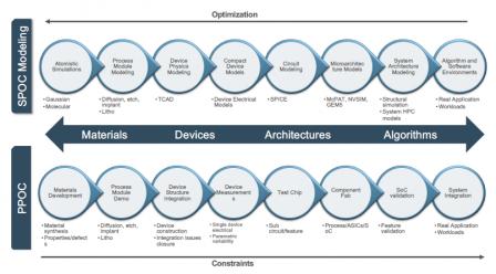
Figure 7. Materials, TCAD, and System co-optimization, using a “Physical Proof-of-Concept” and “Systems Proof-of-Concept” diagram
The power/performance/cost of neural network computation will define how quickly the emerging AI applications will be adopted, in automotive, medical, industrial, aerospace, and consumer markets. It will require re-evaluation of some of the long-standing principles of our industry. The introduction of new memory technologies and the willingness to explore non-traditional architectures offers an interesting development opportunity.
-chipguy
Share this post via:
![SILVACO 051525 Webinar 400x400 v2[62]](https://semiwiki.com/wp-content/uploads/2025/04/SILVACO_051525_Webinar_400x400_v262.jpg)


Comments
2 Replies to “Advanced Materials and New Architectures for AI Applications”
You must register or log in to view/post comments.