With advanced semiconductor processes continuing to shrink, the number and complexity of parasitic elements in designs grows exponentially contributing to one of the most significant bottlenecks in the design flow. Undetected parasitic-induced issues can be extremely costly, often resulting in tape-out delays.
Silvaco addresses this challenge with its EDA tool, Viso, which enables intelligent exploration of parasitic effects. Viso helps designers identify and resolve the root causes of parasitic-induced issues early in the design cycle, significantly improving design reliability and reducing time-to-market.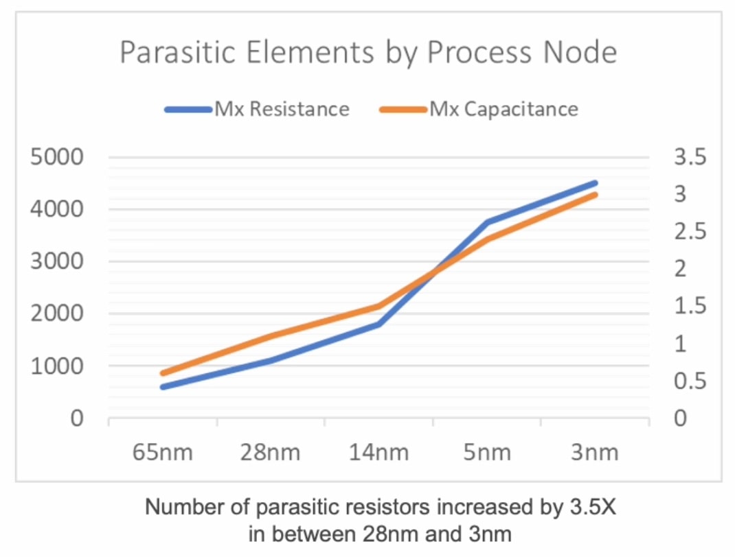
Carlos Augusto Berlitz, PhD , Corporate AE at Silvaco presented a webinar on their Viso tool, so here’s what I learned about its features for parasitic exploration, analysis and debug:
- RC Delays and Resistances: global node-to-node and detailed calculation
- Net-to-Net Coupling: sensitive nets verification, coupling map
- Net comparison: Resistances, RC delays, Coupling capacitances
- Sanity Checks: DC path, instances, dangling nodes, etc.
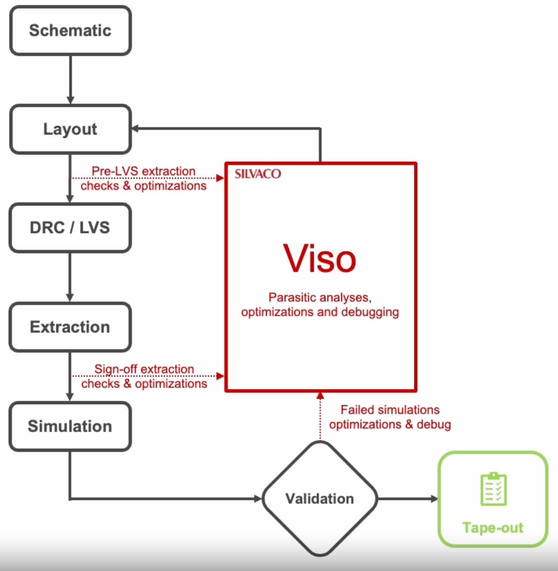
Users can find detailed information about their parasitics, like layer contributions, a heatmap for visualization, tables and charts. You don’t have to resort to time-consuming manual analysis approaches and excessive SPICE simulations.
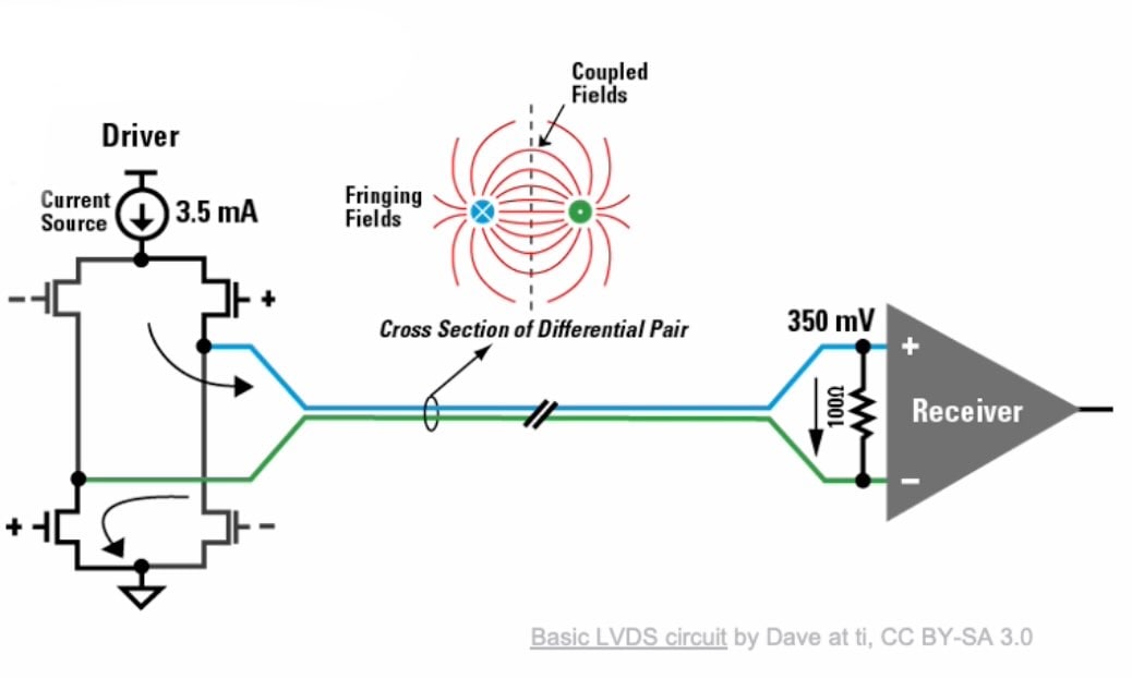
Carlos demonstrated Viso with an example high-speed circuit for LVDS operating at 1.2V where a differential signal is used to reduce electromagnetic noise.
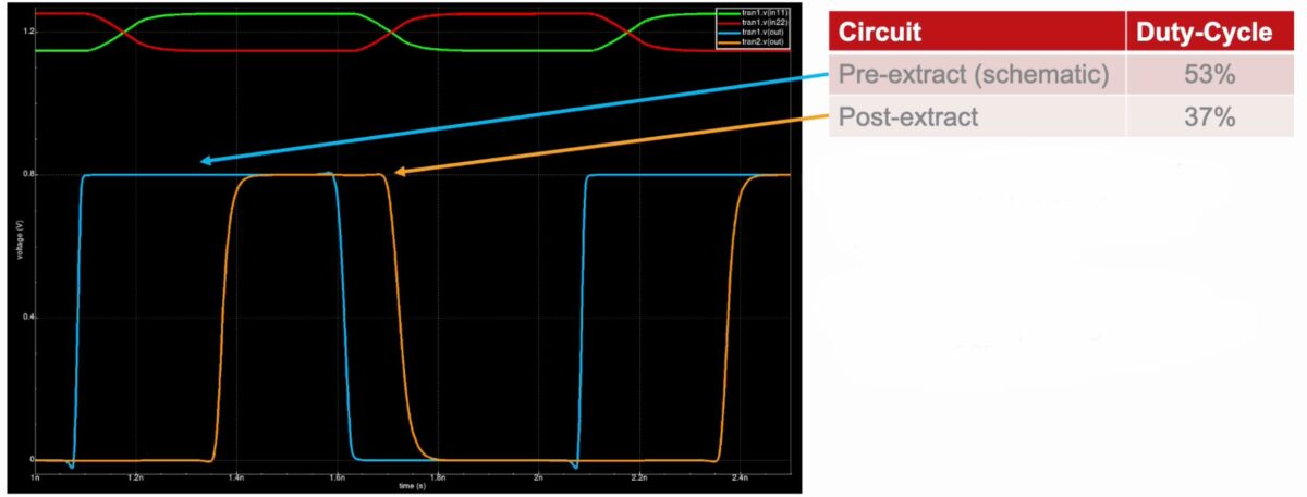
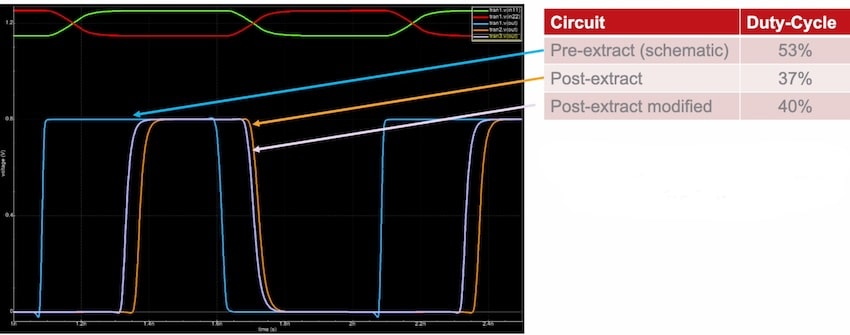
Comparing the pre-layout netlist versus post-extracted simulation shows that the duty-cycle had been degraded, so the challenge was to find out how to make the duty-cycle more balanced. Shown in blue is the plot of the schematic netlist with a 53% duty-cycle, and the orange plot is from the post-extracted netlist with a 37% duty-cycle.
Viso was used to look at different nets in the path of the input signal to the output to determine the biggest net contributors to RC delays. Here’s the cumulative RC delay on four nets in the path, where blue is the shortest delay and red is the longest delay.
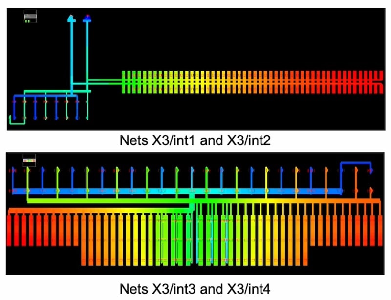
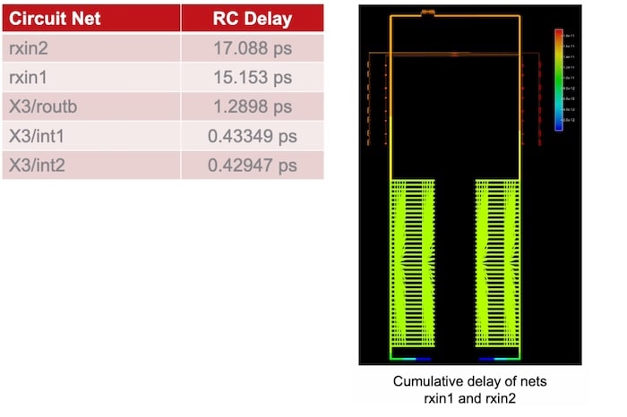
Once a net has been identified, the tool further shows the highest contributors to the path delay, speeding up the analysis process, all without having to run a SPICE circuit simulator. Tool users can visualize the main layer contributors in tables and charts and even see how sensitive the results are to changes in each layer.
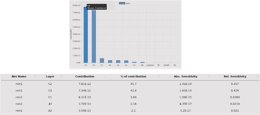
Diving deeper, the tool shows parasitic resistance by each layout segment, so designers and layout engineers know exactly what in the layout is contributing most to RC delays. Knowing where in the layout the largest RC contributors are located allows them to make corrections with precision and fewer iterations. The what-if feature allows you to recalculate the analysis quickly to explore the impact of fixes all without changing the layout. Based on the RC analysis so far, a layout change was made and then the parasitics extracted, yielding an acceptable improvement to a 40% duty-cycle.
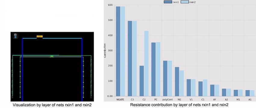
Another useful feature in Viso is comparing two nets to verify that they are matched by parasitic resistance, RC delay or capacitive couplings. Differential pairs with imbalances can be quickly spotted. From the example LVDS it was discovered that the RC delay and parasitic capacitive couple were balanced on nets rxin1 and rxin2, but the balance of parasitic resistances between both paths could be improved as shown in the resistance path comparison plot with red points.

The resistance contribution of layer C2 between nets rxin1 and rxin2 were not balanced, identified by Viso in the bar chart comparison.
Capacitive coupling between nets can also be compared to see how it impacts RC delays. When you need to balance capacitive coupling, this is a quick method to use. Another useful feature is analyzing capacitive coupling comparisons by aggressor nets, something not easy to do with traditional parasitic analysis methods.
Summary
With the newer approach using Viso your team can perform analysis of parasitic effects more thoroughly, in less time, with fewer resources and fewer iterations. Using Viso allows engineers to debug and fix parasitic issues early, thus reducing lengthy design cycles. Finding key layout segments where parasitics limit performance is now possible, even tasks like parasitics balancing and matching of differential signals and differential pairs becomes feasible. IC design teams will benefit by adding Viso to their tool flow.
Watch the archived webinar online.
Related Blogs
Share this post via:
![SILVACO 051525 Webinar 400x400 v2[62]](https://semiwiki.com/wp-content/uploads/2025/04/SILVACO_051525_Webinar_400x400_v262.jpg)


Comments
There are no comments yet.
You must register or log in to view/post comments.