No single EDA company provides all of the tools needed to define requirements, design exploration, track IP, simulate, manage and verify a complex SoC system, so it makes sense that EDA vendors and point tool companies have tools that work together to achieve all of these difficult tasks. Systems design has been around for decades and has been enabled by the widespread use of Product Lifecycle Management (PLM) tools that help manage the process of starting with an idea then tracking details through the end of life. Our modern lifestyle is only made possible through huge industries that already use PLM systems: automotive, aerospace, IoT and consumer.
Some of the common features of a PLM system include:
- All product data and metadata are easily accessed
- Collaboration happens when people and processes all access the same data
- Instant access to data speeds decision making
Our own semiconductor industry caught hold of the PLM concepts first from the mechanical CAD companies looking for new markets, so they really focused on “part” management and some design process data. As you can imagine these first PLM systems were not widely adopted at semiconductor companies, but the good news is that PLM systems have grown over time to include product Bill Of Materials (BOM) plus the data needed for design and verification processes.
Chip design firms are big re-users of semiconductor IP which have created a fast growing market opportunity for IP vendors to serve along with verification IP, so that both design and verification schedules are sped up. These IP building blocks can be well documented, quick to deploy, and are designed to meet industry standard specifications, aspects which quicken time to market. With this new IP reality we need PLM systems that can track semiconductor IP across global borders and dispersed design teams.
Going back to an idea in the opening paragraph, there are incentives to integrate a PLM tool at the system level along with a semiconductor IP lifecycle management tool, creating a coherent process across the entire product lifecycle. Such an integration enables a team to start with an idea, define requirements and trace that all the way through detailed SoC implementation. Even the team members in manufacturing, sales and support are included in this PLM environment. For IP Lifecycle Management we create a new acronym – IPLM.
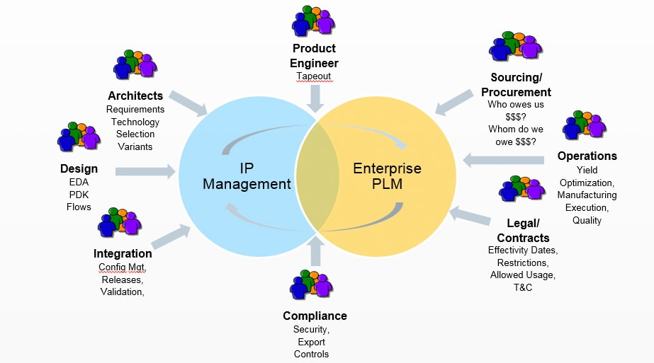
Let’s stop and think for a moment about how some organizations have been separated into distinct departments, with narrowly defined tasks, then each department chooses to use tools that make sense for their separate area which then causes data silos to emerge where valuable data isn’t visible or being shared between departments. See if this disconnected, two-silo approach looks familiar to an organization you may have worked in before:
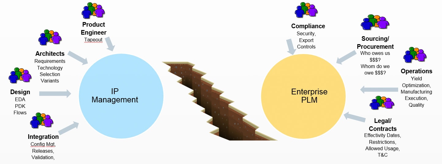
In this product flow we have have two distinct groups that are not connected because their tools are in silos:
- Product Engineers, Architects, Designers, Integration Engineers
- Compliance, Sourcing/Procurement, Operations, Legal/Contracts
Now let’s turn to an enterprise that uses integration between IPLM and PLM technologies to see how an idea gets started and followed throughout a complete product lifecycle, something that spans multiple departments and many stakeholders:
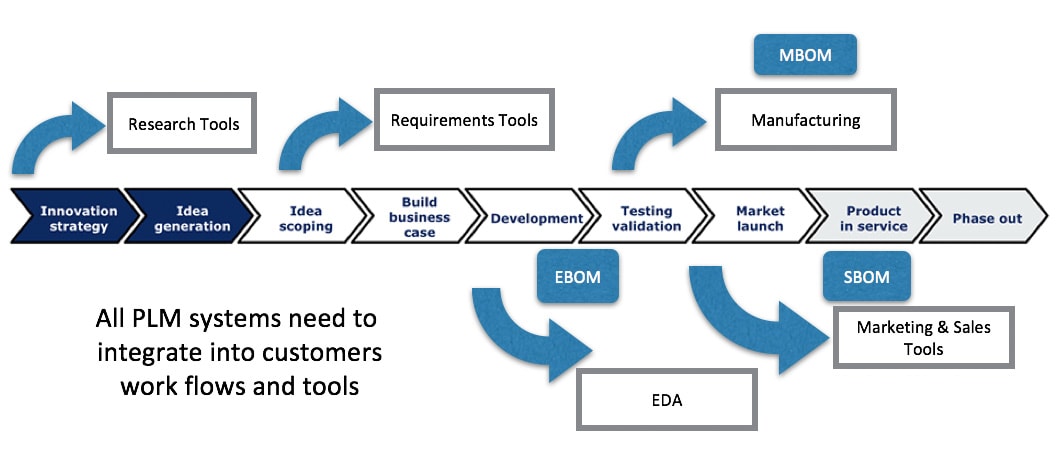
With this integrated approach each group receives their unique BOM: engineering, manufacturing, service. Continuing to drop down into the development box, this is where traditional EDA tools and IP blocks form an SoC design flow, resulting in silicon wafers and packaged parts:
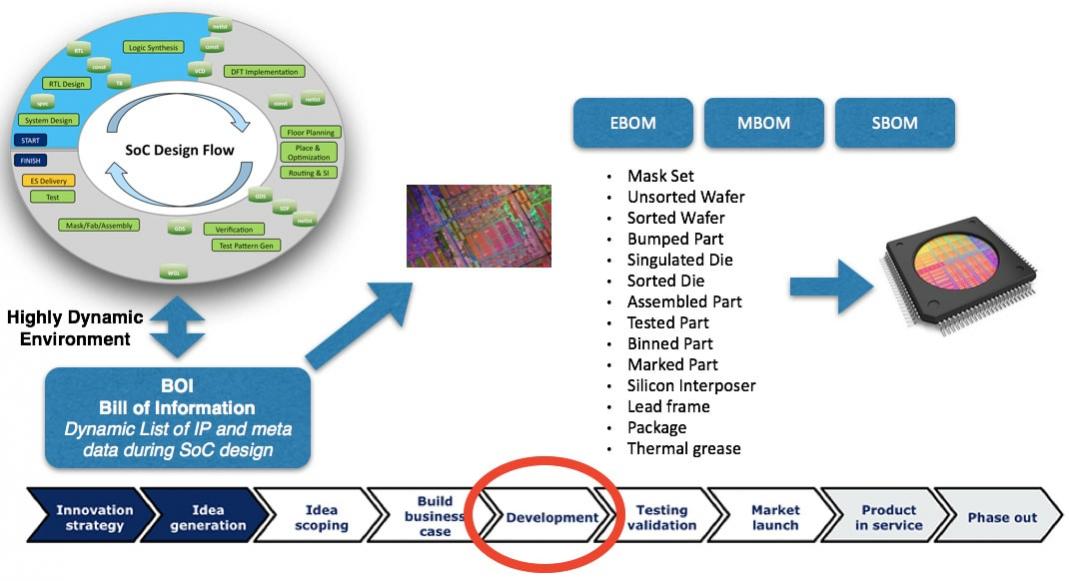
All of the design details used to create the SoC can be labeled a Bill Of Information (BOI), which includes each semiconductor IP block along with all of the metadata. The ideal IPLM system should work with common environments:
- Source Code Management – SCM integration (Perforce)
- Linux command line
- Analog IC tools (Cadence Virtuoso)
An EDA company named Methodicsdoes offer such an IPLM tool, dubbed Percipient that allows teams to perform IP lifecycle management, enables IP reuse, and provides an updated IP catalog throughout the IC design process. Each member of the chip design team can decide which version of a particular IP block they want to incorporate into the portion of their design hierarchy.
The Percipient tool has the concept of ‘workspaces’ where creators work in, created by the SCM tool, then managed by Percipient. Users of each IP block would have ‘read-only’ workspaces created from the SCM tool, and then decide which version of the IP to use. Here’s a diagram of how Percipient works with an SCM and other tools:
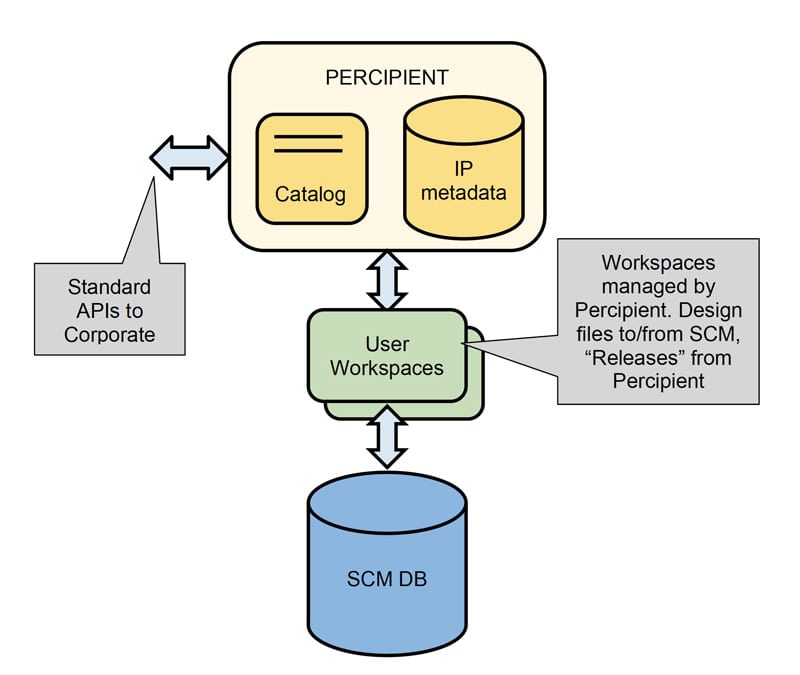
IC designers could just try and package an IP block with maybe hundreds of files and folders into a simple tarball, but that approach is quite inefficient as IP blocks start to reach GB file sizes, IP tracking isn’t part of a tarball, making fixes to an IP block would mean re-tarring and distributing to all users, and knowing what changed between versions is difficult with a binary tarfile. So in each of these cases the optimized approach in Percipient is much preferred.
Engineers love efficiency, so Percipient includes a command line client in Linux that is quick to learn: catalog listing, workspace operations, releases, tracking, etc. Commands can take a JSON argument so that you can view output results in JSON. Here’s an command line example to look at an IP tree hierarchy:
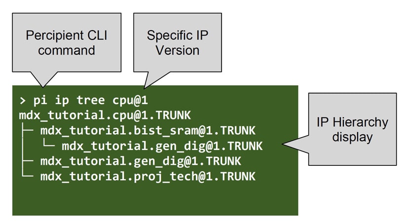
Team members can even code in their favorite language (.NET, Python, Perl, C++, etc.) or framework that supports GET and PUT requests to URL endpoints, controlling Percipient with an API.
Percipient manages IP hierarchy for blocks that use digital, analog and mixed-signal designs, along with version control. Each IP block can include rich data like graphs, charts, even HTML data sheets. Chip designs can query the IP catalog to find each IP block best suited for their project.
Engineers at Methodics have figured out how to integrate their IPLM tool with any PLM system using a set of four integration touch points as show in the following diagram:
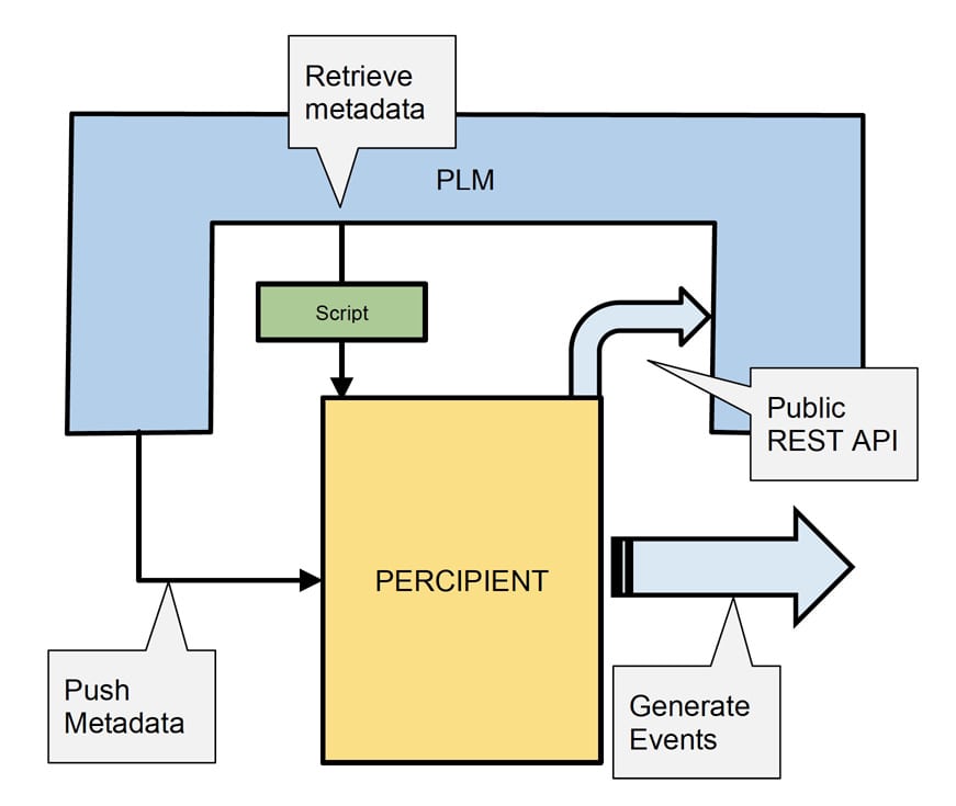
So the good news for SoC design teams is that they can continue to use their favorite PLM system along with the IPLM from Methodics in an integrated fashion, creating a seamless flow, which in turn has improved communication within the team, shortening product development cycles in your enterprise.
Summary
Semiconductor design companies can now create new systems more efficiently and with fewer errors and iterations by taking an integrated approach with their PLM and IPLM tools. Methodics has led the way in enabling such an integration with their IPLM tool and they have the experience integrating with other PLM vendors. To learn more about this topic consider reading the 20 page White Paper from Methodics – Putting the “I” in PLM.
Related Articles
- SoC Design Management with Git
- Hierarchy Applied to Semiconductor IP Reuse
- Rethinking IP Lifecycle Management


Comments
There are no comments yet.
You must register or log in to view/post comments.