There’s a lot to unpack in the title of this post. First, Siemens EDA is the new name for Mentor, a Siemens Business. The organization continues to operate as part of Siemens Digital Industries Software. The organization has released a white paper that describes research done with the American University of Armenia. The work examines how to use machine learning (ML) modeling techniques to predict wafer surface topography after a back-end-of-line metal deposition step. It’s critical to get these predictions right so chemical mechanical polishing (CMP) can do its job effectively. Read on to see how Siemens EDA is applying machine learning to back-end wafer processing simulation.
Smoothing Out the Bumps
This is a story about smoothing out the bumps in wafer processing. Many of the process steps in chip manufacturing need a smooth surface on the wafer to ensure patterns are printed correctly during photolithography. These patterns form the devices for the chip and they’re very sensitive to distortion that can be caused by a non-planar (bumpy) surface. I’ll get into where these bumps come from in a moment. The method to smooth the surface is accomplished by the previously mentioned CMP step, which is quite complex.
During CMP, a polishing pad is pressed against a rotating wafer and a mixture containing abrasive particles and chemicals is injected between the pad and the wafer. Mechanical and chemical interactions occur at the wafer pad contact area, removing material from the wafer surface to smooth out the bumps. If you’re thinking this sounds like polishing your car, it’s a whole lot more complex than that. The pressure applied by the pad and the makeup of the chemicals injected all influence the quality of the result. Material is being manipulated at a microscopic level across the wafer surface to achieve maximum planarity (i.e., smoothness).
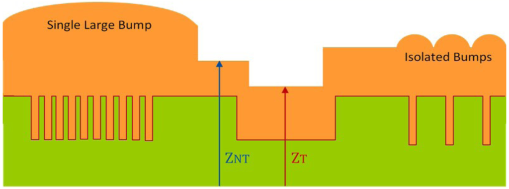
Back to the bumps. Where do they come from? This part of the story is about metallization, that is, creating the interconnect for the chip. Copper is deposited on the wafer surface using an electrochemical deposition process (ECD). This is another highly complex process that uses a variety of chemicals to minimize bumps, based on the underlying surface that the metallization is being deposited on. While these approaches can help, bumps happen, and the CMP step is required. The figure below illustrates a typical profile after ECD and before CMP.

For all this to work, an accurate prediction (through simulation) of the post-ECD surface is needed to drive the simulation that is used to set up the CMP process. During the first part, i.e., the simulation of the post-ECD surface, machine learning finds useful application.
How Machine Learning Helps
To model and simulate the ECD process, the design is first divided into fixed-size tiles. For each tile, average values of geometrical characteristics like width, space, pattern density, and perimeter are extracted. A series of complex mathematical models is then applied to each tile. After the analysis completes, the surface profile data for each tile are used as input for the CMP model. This is a long and complex process, and this is where neural networks from the field of machine learning find application.
A fully connected neural network-based full-chip deposition model for predicting the post- deposition surface profile is described in the white paper. Multiple ML algorithms are used to address the complicated surface variation that is typically seen. A key part of ML is applying large data sets of known results to “train” the neural networks. The white paper describes a series of experiments using Calibre® CMP ModelBuilder and CMPAnalyzer tools. First, physics-based models using data collected at the factories are created. These physics-based models are then used to generate the training, validation, and test data for ML model building.
The white paper then describes the application of various methods to find the best combination of run time and accuracy. The best methods exhibited a much shorter training time (a couple of hours) compared to other methods (several hours or several days). The ultimate results showed improved accuracy with lower run times compared to more traditional approaches. The post-ECD surface is also influenced by shapes that are not close by and ML approaches helped to model these longer-range effects as well.
ML is clearly finding its way into many applications. This is another example. You can access the full white paper, entitled MODELING ECD WITH MACHINE LEARNING FOR CMP SIMULATION here. Check it out to see how Siemens EDA is applying machine learning to back-end wafer processing simulation.
Also Read:
CDC, Low Power Verification. Mentor and Cypress Perspective
Multicore System-on-Chip (SoC) – Now What?
Share this post via:


Comments
There are no comments yet.
You must register or log in to view/post comments.