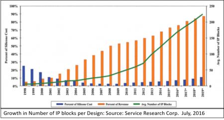
 I recently wrote an article about networks-on-chip (NoC) and how Systems-On-Chip integrated circuits (SoCs) are becoming increasingly more complex and heterogeneous in nature. While researching for that article I came upon a new micro-site by Dassault Systemes that goes into great detail about the operational challenges faced by the semiconductor industry in its reuse of intellectual property (IP).
The site gives a good description of how the Internet-of-Things (IoT) is simultaneously pushing the market towards shorter design cycles while increasing the demand for SoC customization, effectively putting solutions providers between a rock and a hard place. The industry has responded to these diametrically opposing requirements by leveraging IP reuse with an estimated 200+ IPs now used per SoC.

As mentioned the in previous article these SoCs are driving to more heterogeneous content with the implication that the semiconductor companies are now dealing with a tremendous IP management burden. Dassault Systemes new micro-site addresses the challenges of Enterprise IP Management with three phases as shown below. Posted on the microsite are three white papers, one for each of these phases, and I would encourage SoC designers to read them as they do a good job of outlining what is required to be successful in this new world of hyper IP-reuse.
The first white paper is entitled, ‘Creating a Solid Semiconductor IP Foundation’ and covers the challenges of scaling and sharing IP at the enterprise level. This paper includes such topics as IP cataloging, IP governance and IP defect/issue tracking. The paper points out that companies have done a pretty good job ‘below-the-line’ in the details of their technical design activities. The problems however start appearing as tasks move ‘above-the-line’ to the enterprise level. This is especially true for larger companies that have multiple globally diverse teams that are expected to develop and share IPs in addition to doing their regular design work.

Many years ago I was a CAD engineer in Texas Instruments’ ASIC division. We were just at the beginning of real design reuse and I can distinctly remember the first time one of our customers took a TI DSP core and used it as a cell in their ASIC design. The jump in our customer’s productivity was huge as they took advantage of all of the man years TI had invested in their custom DSP development along with the automation we in the ASIC division had wrapped around the design and test flows.
It was technically challenging for us at TI as it required us to work across multiple enterprise boundaries to make the customer successful. The DSP and ASIC groups were two separate business units with different ways of dealing with practically everything, including design, packaging, test, business models and even legal requirements.
In the end our efforts for the customer were successful but we did not yet have a scalable process that could be easily repeated. We proved it could be done but at the time we lacked the basic infrastructure and tools required to do this type of IP reuse efficiently and with predictable results. It was, however, a wake-up call that our standard product businesses were at risk as we suddenly saw how competition could quickly enter into our markets with highly differentiated and customized products.
 As I read Dassault Systemes first white paper I related with all of the issues they discussed around the scaling and sharing of IP at the enterprise level. As a CAD engineer, I especially remember the simple things that got in our way. Examples of this included the different vocabulary used by the ASIC and DSP design groups as well as the dramatically different design flows used by each.
After reading the first white paper I also realized just how far the industry has come since those early days at TI. The white paper does an excellent job of detailing the issues and requirements for IP cataloging, IP governance and IP defect & issue tracking as laid out by the ‘early-phase’ of their IP management model. More importantly, the paper introduces the reader to solutions for those issues including a brief introduction to their ENOVIA product life cycle management solutions.
As the semiconductor industry evolves into a more multi-discipline, collaborative ecosystem that requires the efficient reuse of design IPs from multiple sources (both internal and external to the organization), it’s clear that a concerted effort will be needed by solutions providers at both the technical and business levels to work with sophisticated tools for managing IPs across the entire enterprise. Dassault is leading the way. Take a look at the white papers and keep an eye out for additional blogs on this topic in the upcoming weeks.
The Dassault micro-site can be found here: http://www.3ds.com/industries/high-tech/ip-management/
The link to the white paper is here, Creating a Solid Semiconductor IP Foundation.
See also: ENOVIA Solutions
Factors Affecting the Future of the Semiconductor IP Management Business


Captain America: Can Elon Musk Save America’s Chip Manufacturing Industry?