As every other person is talking about IoT today, Michael Munsey of Dassault Systemes looks at this trend in the context of critical success factors and Dassault’s strategy towards providing semiconductor solution that integrates the design chain and continues to keep the semiconductor eco-system healthy and profitable. I looked at one of his presentations to his top customers where he draws the inference of changing world from 1 device for 1000’s users in 1960s to 100’s of devices per single user in near future, what will drive such devices, what are the gaps and how those gaps can be filled. Let’s see in a brief what this means.

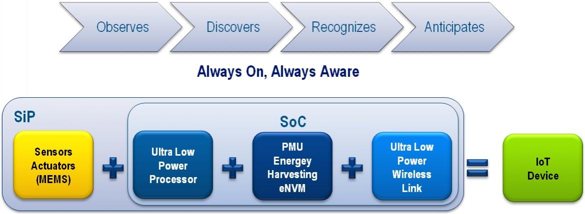
A device for IoT will be a new class of device which will have sensors, actuators and SoC containing ultra low power processor, wireless link and power management units, all in the same package. This device will be intelligent enough to sense, analyze, anticipate and act, and will be always on.
Clearly, all of this cannot be done by one single vendor in a captive way. In order to bring excellence in all parts of the product, there needs to be design creators to bring fastest, smallest and lowest power IPs and design integrators to provide robust integration platforms for SoC implementation to bring out high quality products at right cost and right time. So, what is the gap we are talking about?

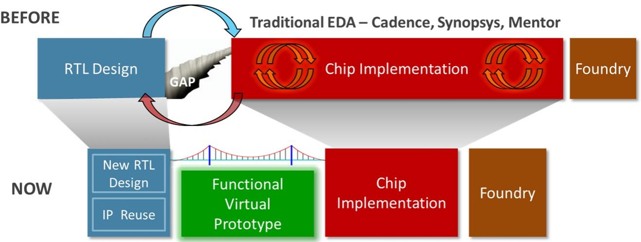
The gap comes at the time of integration of all pieces together. How do we know the final product will come in perfect order as we desired while all components come from diverse sources with lot of heterogeneity involved between them? To fill that gap, from a system’s perspective, a seamless handoff between RTL design along with IP reuse and chip implementation is needed and that can be filled by functional virtual prototyping. A functional virtual prototype between RTL and chip implementation can rightly estimate the power, performance and area before the final implementation can proceed, thus eliminating rework, shortening design cycle and meeting time-to-market. How can Dassault contribute in filling this gap faster and more precisely which can lead to a profitable business?

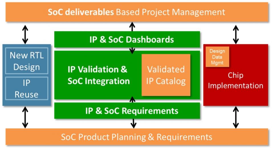
If you look at Dassault’s semiconductor strategy (From Productivity to Profitability) in one of my previous article, there are couple of steps between Product Engineering and Design Engineering which ensure requirement specification based management and New Product Introduction (NPI) based on what customer needs, and then IP management, protection, integration, design and validation. So, here during virtual prototyping, SoC deliverable based project management, requirement tracking and planning can be done. Dassault provides Validated IP Catalog management which can trace a best suited IP for a particular requirement and readily present its properties, thus aiding in faster and appropriate IP integration into SoC. During chip implementation, Dassault provides its versatile Design Data Management support.
Also, Dassault’s SRDV (Semiconductor Requirement Driven Verification) solution provides capability to track SoC verification and validation results back to SoC’s requirements. Read more on this in the article – Dassault’s Simulation Life Cycle Management.
It looks like Dassault is on the right toes to support the IoT bandwagon and fetch profitable rewards from there.

More Articles by Pawan Fangaria…..
Share this post via:


Chemical Origins of Environmental Modifications to MOR Lithographic Chemistry