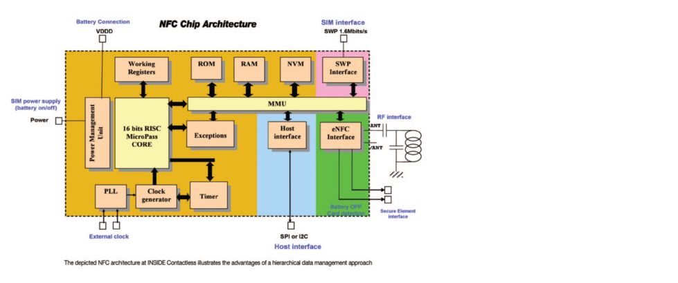
Considering the technological progress, economical pressure, increased outsourcing and IP re-use, semiconductor industry is one of the most challenged industry today. Very frequently products get outdated leading to new development cycles. It becomes very difficult and costly to build the whole scheme of data foundation once again. A systematic management of design data and its re-use is a must in order to manage such frequent changes in product designs, thereby maintaining and improving economic health of the organization.
Last month I wrote about DesignSync, a robust design data management tool and its multiple advantages. Digging further into that data management methodology, I found about how INSIDE Contactless (an innovative company involved into designing chips for payment, access control, electronic identification etc.) used hierarchical design management methodology, offered by Dassault Systemes in its DesignSync tool, to turn a difficult situation involving scattered design data and IPs on different databases across multiple teams, spread across remote sites, into an opportunity with unified data management, leading to success in the business.
INSIDE used design tools from Cadence and Design Data Management (DDM) tool from Dassault, synchronized them to cater to modular data abstraction within the context of hierarchical configuration management and obtained excellent team collaboration across multiple sites resulting into productivity and time-to-market.

The concept of static and dynamic HREF (hierarchical reference) enables creation of multiple design modules and hierarchies under a root design that helps in bringing controlled flexibility and parallelism in the design development process with a unique database for the overall design and strict control on overall integration before release. The project hierarchies can also contain software, document, scripts and IPs from various sources with different time stamps along with the design data. The data repositories worked upon by particular teams can be placed at strategic locations to reduce network traffic. It’s a client – server platform with servers nested hierarchically at multiple sites.
The design is hierarchically built up with lowest unique abstraction of data called as “module” that has consistent collection of files and folders and has access commands like check-in, check-out and modify. Revision history is maintained at each level. HREFs connect modules and are processed when design data is fetched into the workspace. It provides a systematic automated integration of design under a unified Design Data Management (DDM) system which can be either single or distributed.
Dassault provides static and dynamic work flows – “SITaR” (Submit, Integrate, Test, and Release) and “Golden Release”. INSIDE used “SITaR”, that is suited for static HREFs referring to a specific release, at the time of tapeout when design and simulation are done on the baseline data. And “Golden Release” during development phase, where tags like “in development”, “Ready4Use”, “Golden” etc. were used on dynamic HREFs. This labelling on the hierarchical structure gives the integrator strict control over data. He/she can validate and integrate the static data efficiently without any delay. A detailed methodology can be found in Dassault’s whitepaper here.
This methodology fits well into the strategy for semiconductor PLM about which I had written earlier. This helps in efficient data management, intelligence build up for work estimation, scheduling and execution, cost estimation, and efficient and effective re-use of IPs to meet the challenges of SoC design and business.
Share this post via:


Musk’s Orbital Compute Vision: TERAFAB and the End of the Terrestrial Data Center