Semiconductor companies are looking for ways to keep their business profitable by managing expenses on both the design and test side of electronic products, which is quite the challenge as the trends show increases in test pattern count and therefore test costs. Scan compression is a well-known technique first created over 15 years ago that can be used to reduce the cost of testing ICs by compressing your test patterns so that you use less time on the tester and can implement with fewer test pins. Engineers at Mentor Graphics were early pioneers offering compression technology used inside of ICs with a product called Tessent TestKompress.
Just this month the graphics chip company Nvidia announced their Volta GPU with a staggering 21 billion transistors, so Moore’s Law continues to hold up with many special-purpose chips like this one which drive the test challenge. The earliest IC fault model starts with stuck-at, however with smaller geometries we need to add more fault models, like:
- Transition faults
- Path-delay faults
- Multiple-detect faults
- Bridging faults
As more fault models are added it grows the size of test patterns. From a practical viewpoint the number of pins on SoCs has been growing in a linear instead of exponential fashion over time, which then means that the bandwidth for test patterns is reduced. If we can reduce the total number of pins on an SoC, then we can use less expensive test equipment and keep our costs in check.
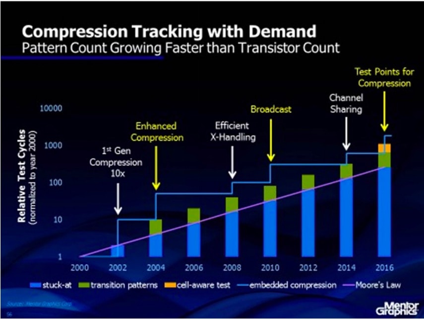
The economic benefit of using a technology like Tessent TestKompress is that it reduces overall test costs by using fewer test patterns, running in fewer test cycles, yet producing a high test coverage metric. Compression really does decrease the volume of tester data while using fewer test channels. Fortunately for our industry the advances in test compression have gotten ahead of the growth curve for Moore’s Law (purple) as shown below.
The acronym LPCT was created to stand for Low Pin Count Test, and it’s a driving factor in keeping test costs manageable in the DFT (Design For Test) world. Reasons for using LPTCT can be summarized as:
- Better top-level chip routing
- Minimizing the total number of pins
- Including hierarchical ATPG
- Lowering ATE costs
- Keeping yield high during wafer testing
- Enabling multi-site testing
LPCT Approach
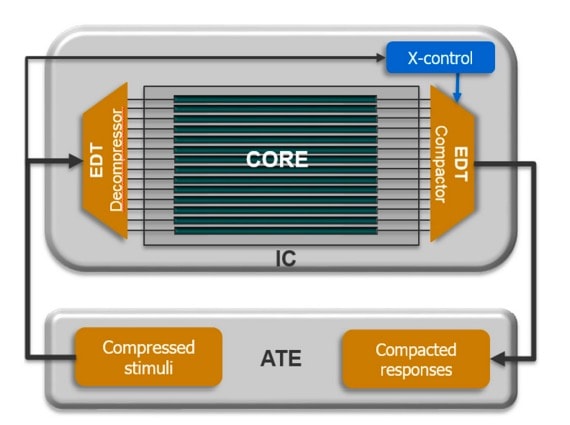
The architecture of Tessent TestKompress has compressed stimuli coming into an IC from the left-hand side where the on-chip hardware decompresses the patterns for testing the core, then the output results from the core are compacted on-chip before being sent back to the tester on the right-hand side.
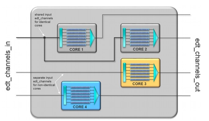
Parallelism in your hardware design can be taken advantage of during test by re-using input stimulus to identical cores as shown below with cores 1 and 2, while cores 3 and 4 are different from each other and therefore still require separate input channels:
During manufacturing test even with compression in TestKompress you still get diagnostics for failing devices without needing offline application of bypass patterns.
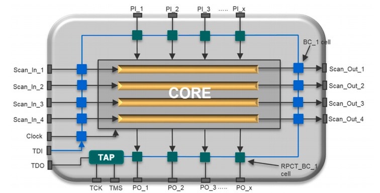
Test pin count can be reduced by replacing the primary IO cells with a boundary scan version as shown below where the core is loaded with just four scan IN pins, and read out with just four scan OUT pins.
LPCT Controllers
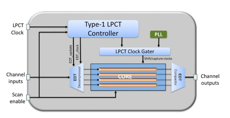
There are three styles of LPCT controllers and each one of them is supported with TestKompress, and the benefit is minimizing the total pin count needed by your tester. Here’s the Type 1 LPCT controller architecture which takes the fewest gates:
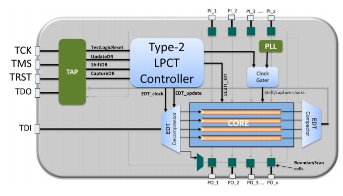
For a Type 2 LPCT Controller we are using a 4 or 5 pin TAP interface which allows us to eliminate connections to the functional I/O pins:
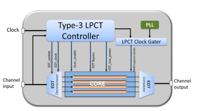
Finally for a Type 3 LPCT Controller we need only 3 digital pins, while the controller uses about 1,400 gates:
Summary
The challenges to growing gate counts on SoCs have pressured the DFT community to come up with compression approaches to keep test times in line. Mentor recommends using LPCT along with their compression called TestKompress as a way to maintain high test coverage with the minimum tester time. The automation with TestKompress allows DFT engineers to be quite productive while minimizing the design changes.
Read the complete 8 page White Paper on this topic online.
Share this post via:


Comments
There are no comments yet.
You must register or log in to view/post comments.