
High-speed digital (HSD) design is one of the more exciting areas in EDA right now, with design practices, tools, and workflows evolving to keep pace with increasing design complexity. With the annual Chiplet Summit and DesignCon festivities right around the corner, we sat down with Keysight’s Hee-Soo Lee, HSD Segment Lead, to get his insights into what’s happening and where engineers should be looking for workflow improvements. What you’ll read next focuses on trends, customer needs, and what Keysight EDA is doing about them. Keysight will present its solutions, including Chiplet 3D Interconnect Designer, at both events.
SW: When we talked last year, we discussed new approaches to automated crosstalk analysis and its role in the first-pass success of more complex 3DHI designs. You’ve learned more about how engineers approach high-speed chiplet interconnects – what’s happening right now?
HSL: Everybody is talking about AI/ML, right? Many design teams are moving in that direction. One area attracting strong interest is advanced package design for high-traffic AI data centers. There are new technologies in play – multi-die, stacked die, heterogeneous integration, hybrid bonding, and more, all in advanced packaging. Packages are becoming faster and more complex, as designers aim to pack more functionality into a single package and save space. It’s turning out that success or failure in these designs largely depends on getting the high-complexity interconnects right.
SW: Sure, multiple 128-bit buses running at 64GT/s rates, what could possibly go wrong?
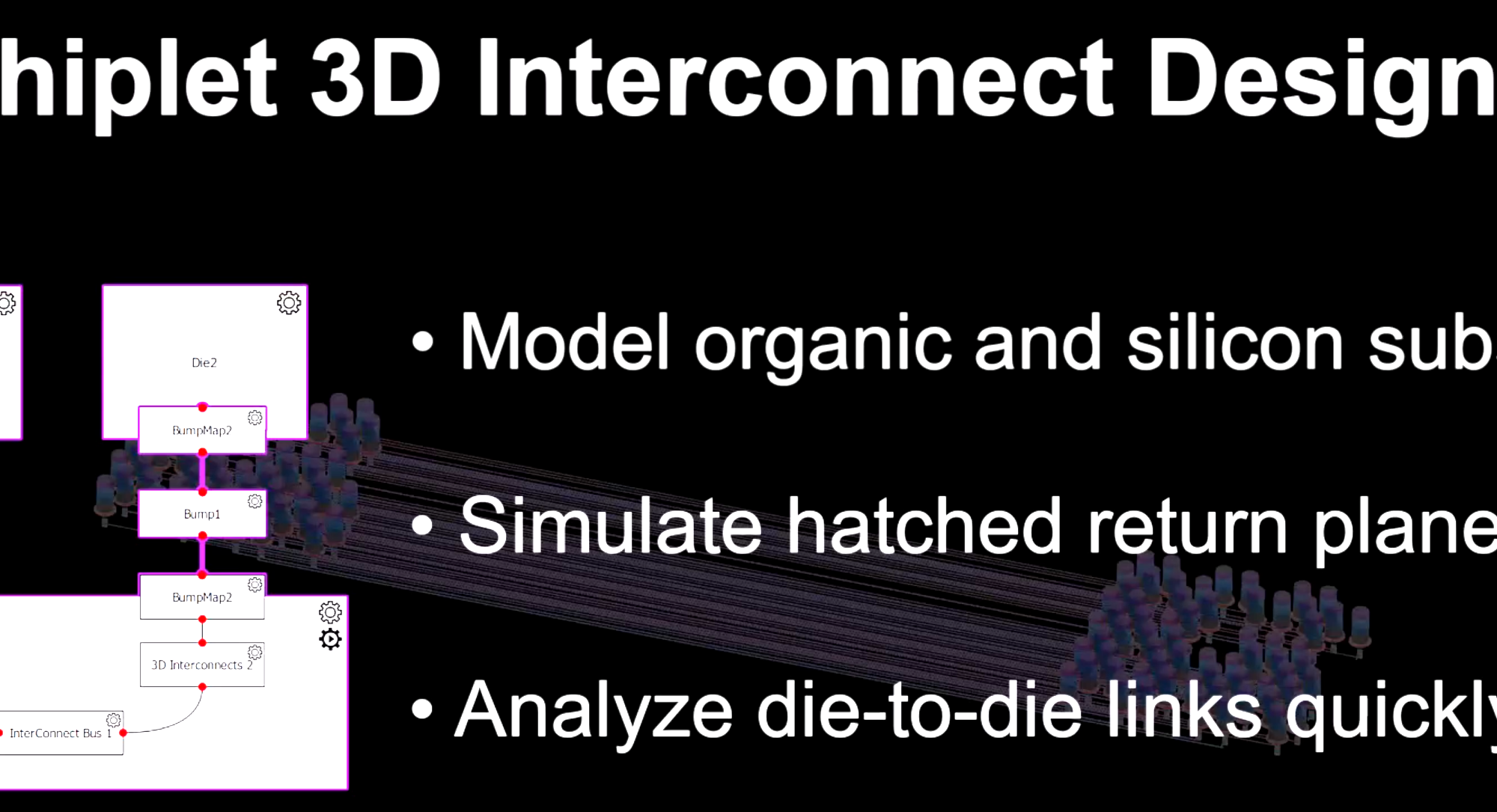
HSL: Exactly. There’s a lot that can go wrong when integrating different functional blocks into a single advanced package. Effects now happen on a 3D landscape. Signal integrity used to mean looking across a bus from source to destination. While bits on a bus may couple to other bits on the same bus, they can also affect other signals in the package, especially given vertical proximity, or part of the bus might be affected by something else. Designers start with “proven” chiplets and integrate them using silicon bridges or interposers, then route signals from those chiplets through physical packaging. Simplistic models don’t work well because every interconnect is a transmission line at these speeds. Signal integrity is a major concern in hatched or waffled ground-plane structures, which are almost mandatory given manufacturing constraints. There are holes in the ground return path, which may increase signal reflection and crosstalk, and this is really hard to model with conventional techniques due to its complexity.
SW: This is way beyond guessing where to place bypass capacitors on a printed circuit board, I suspect.
HSL: Without accurately modeling and simulating parasitic effects of all 3D structures in an advanced package design, there’s no hope to mitigate behaviors with external band-aids on a board. Everything going on inside the package has to be modeled and analyzed – looking at just part of the design and assuming the rest will perform the same way misses problems. However, customers tell us that finding the simplest ground-plane issues can take weeks of analysis, and even then, the analysis still doesn’t provide enough information to fix the more complex problems they’re encountering. It’s bringing traditional workflows to a grinding halt.
SW: So, they’re asking you for help? Modeling and simulation capabilities in Keysight Advanced Design System (ADS), along with new features such as Chiplet 3D Interconnect Designer, can provide a clearer picture?
HSL: Customers told us we need to do something, fast, and we have. We’ve been able to show engineers how to turn a comprehensive analysis of interconnects, including hatched ground planes, from weeks into minutes using Chiplet 3D Interconnect Designer. Imagine visually highlighting problems in a design in a few minutes, making corrections in one or more structures, re-running the analysis in a few more minutes, and seeing better results. Now teams can focus on optimizing the design and validating that it meets specifications.

SW: Or trying to find HBM parts, many of which are now in what vendors call allocation.
HSL: HBM supply is certainly a problem right now for all but a select few customers. You don’t want to be in the position of finding that a design needs to be redone for a different part because the one you specified had its lead time blow up while weeks of analysis was running.
SW: What about keeping up to date with the latest specifications?
HSL: That can be hard, too, and making that easier is a big focus in ADS and companion tools. In the last year, we’ve seen several revisions, including UCIe 3.0, PCIe Gen 7, and HBM4. And to complicate matters, customers sometimes customize their interconnects, borrowing concepts from UCIe or BoW but not adhering to all compliance rules. Faster analysis of the latest revision of pertinent specs or a user-defined set of rules enables our customers to stay competitive at the leading edge.
SW: You’ve coined a fascinating term – “design for hope.”
HSL: RF designers are dealing with a few crucial signal paths. High-speed digital designers are dealing with 128 or more signals between endpoints. Crosstalk analysis has been so tedious that engineers choose to look at only a few signals, get the eye margin where they’d like it, replicate the bus structures, and hope the rest of the lines are OK. As soon as real-world bridges, interposers, and packages appear, there’s a huge risk that the margin on the unobserved parts of the bus disappears. That’s an expensive omission just to save simulation time, yet engineers do it every day, and they pay the price if they miss. We’re at the point where data rates, ground planes, materials, structures, and packaging are unforgiving versus tight margins in specifications.
SW: Speaking of packaging, this workflow also helps there, correct?
HSL: Yes, the days when folks could design a chip and toss it over the wall to the packaging person and expect decent results are over. The classic workflow would perform a post-layout EM extraction, which at least provided some information, but not enough. Advanced packages mandate a co-design strategy with the 3DHI chip and either a bridge or an interposer. When comprehensive analysis runs in minutes, design space exploration, including packaging, yields better results.
SW: What big stuff is looming on the high-speed digital design frontier?
HSL: Power consumption is still a big concern at scale. Large AI chips have broken the 1000A barrier on their DC supply rail, and data center racks are pushing over 35,000A. Any ADCs or DACs in a design are power hogs. A new initiative, co-packaged optics (CPO), replaces electrons with photons, making it much more power-efficient. CPO may eventually flow back through the packages and interposers to the die-to-die interconnect, creating another transition for high-speed digital EDA tools and workflows.
There are, of course, other developments at Keysight EDA in the high-speed digital, power, and signal integrity circles. Teams of engineers, including Hee-Soo, are descending on Chiplet Summit and DesignCon shortly to share additional insights with audiences. Keysight has a resource hub where you can see everything happening at this year’s DesignCon in Santa Clara.
Keysight DesignCon Resource Hub
You’ll find this short introductory video for Chiplet 3D Interconnect Designer among the information there.
Share this post via:


Comments
There are no comments yet.
You must register or log in to view/post comments.